
TEM Products
TEM Grids with Continuous Formvar/Carbon Film
TEM grids with continuous Formvar film stabilized by a thin carbon layer, providing excellent mechanical support and conductivity for routine and biological applications.
TEM grids with continuous Formvar film stabilized by a thin carbon layer, providing excellent mechanical support and conductivity for routine and biological applications.

With continuous pure carbon film, the associated formvar film is removed for speical applications like sample preparation in organic solvents or at high temperature

Overlay of ultrathin (~3 nm) film on holey supporting film, to hold nanoparticles but have minimum background inteference

Standard square mesh TEM grids without support film, designed for general sample preparation and custom coating applications.

Hexagonal mesh TEM grids designed to maximize open viewing area and minimize beam obstruction for advanced TEM applications.

Rectangular mesh TEM grids designed to provide larger viewing areas while maintaining stable sample support.

TEM grids with a central circular aperture designed for maximum open viewing area and support of thin films.

TEM grids with elongated slot openings designed for supporting large sample areas with minimal obstruction.

Double folding TEM grids designed to securely hold samples by sandwiching them between two grid layers.

TEM grids with reference markings designed for easy identification and relocation of specific sample areas.


Self-closing for easier manipulation of small objects, with ultrasharp curved tips

High purity, all materials, customizable shapes and sizes


Cost-effective silicon wafers for photovoltaic and energy applications
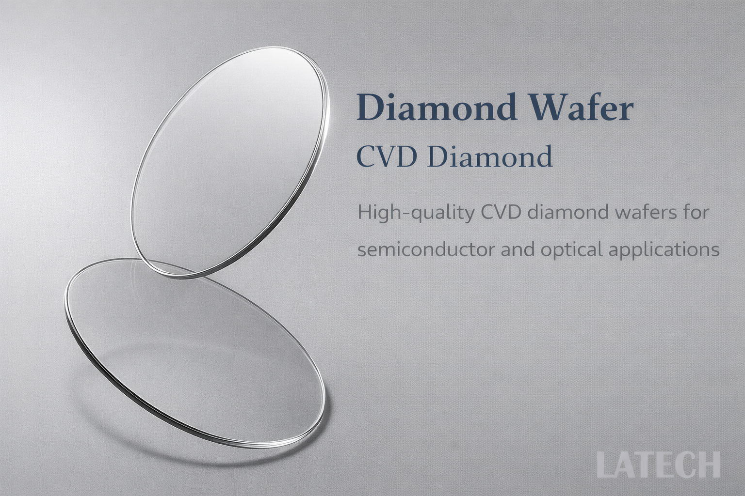
High-performance diamond wafers for optical, thermal, and semiconductor applications.
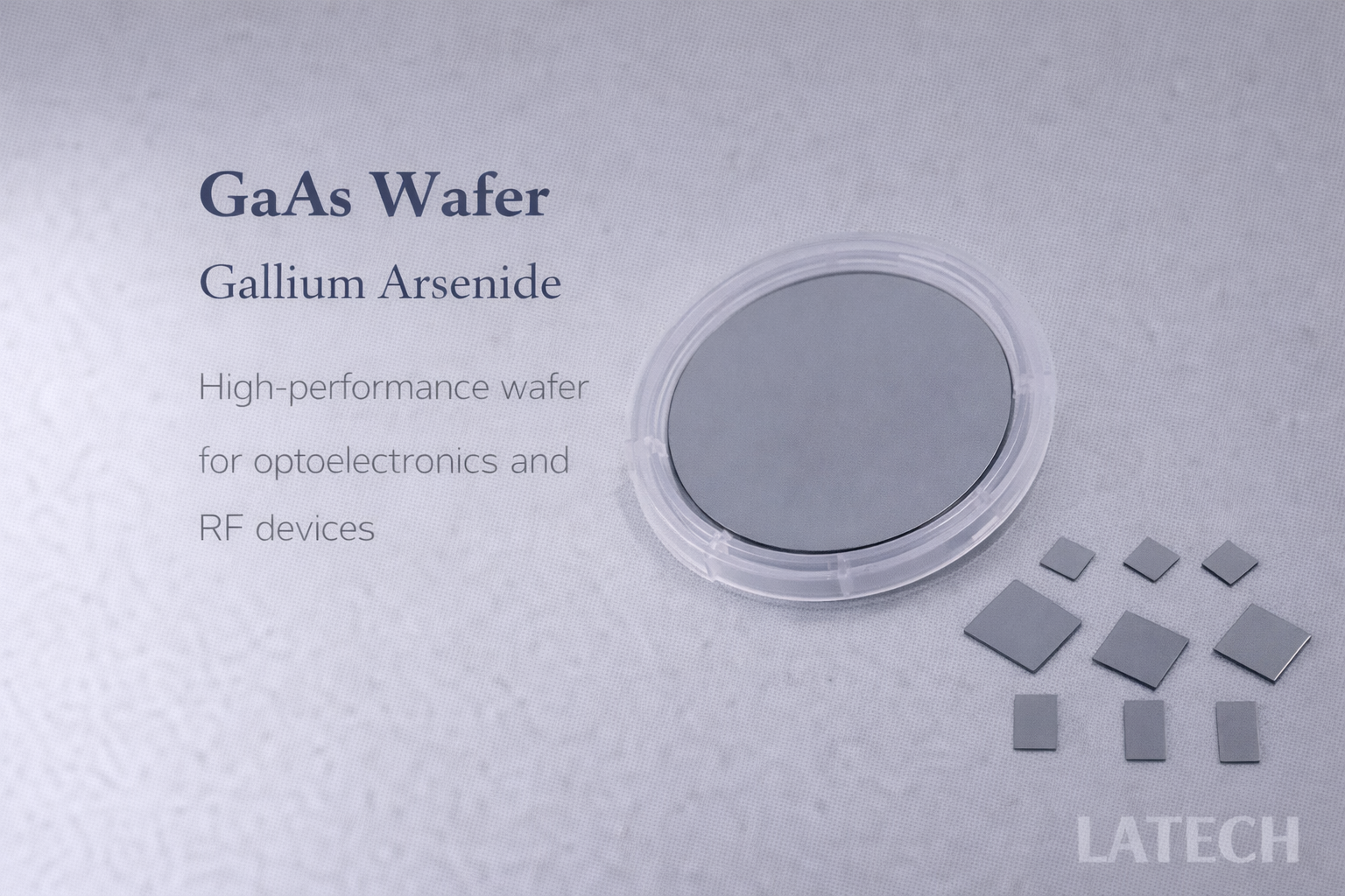
High-performance GaAs wafers for RF, optoelectronic, and high-speed applications.
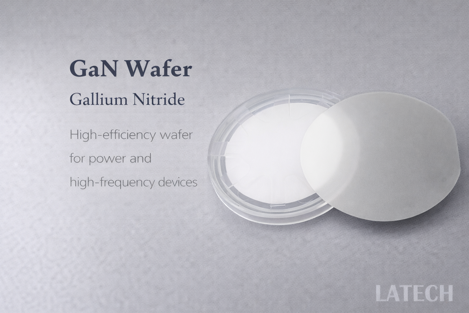
High-performance GaN wafers for power electronics, RF, and optoelectronic applications.
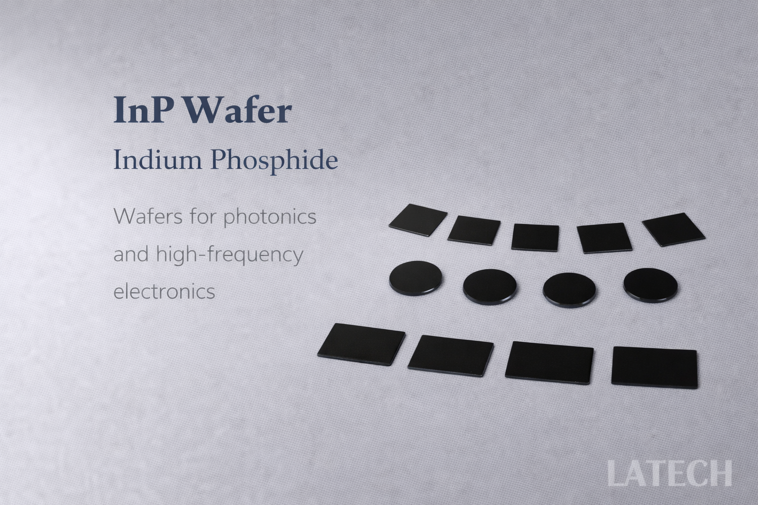
High-performance InP wafers for photonics, optoelectronics, and high-frequency applications.
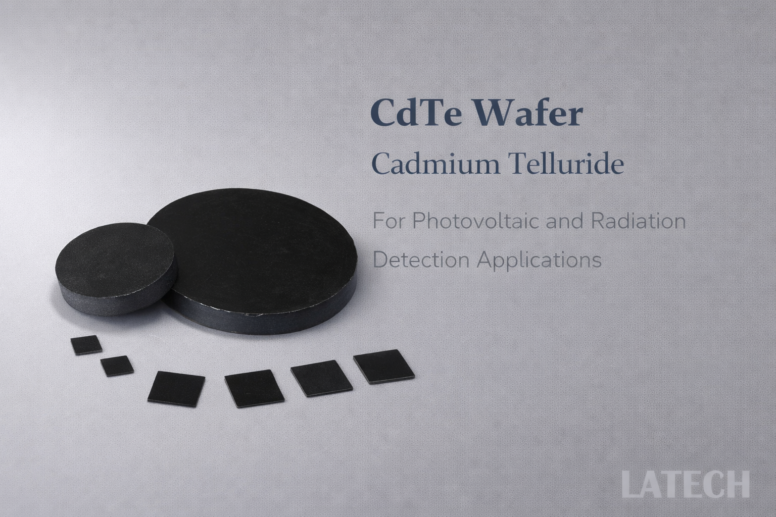
High-performance CdTe wafers for photovoltaic, infrared, and radiation detection applications.
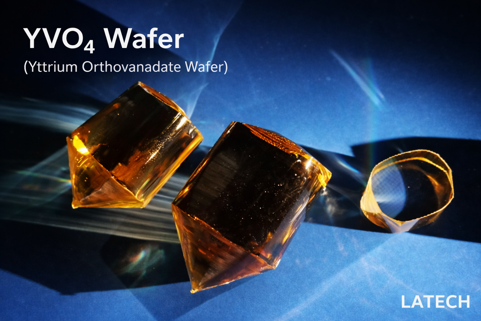
High-quality single crystal YVO₄ substrate for optical and photonic applications
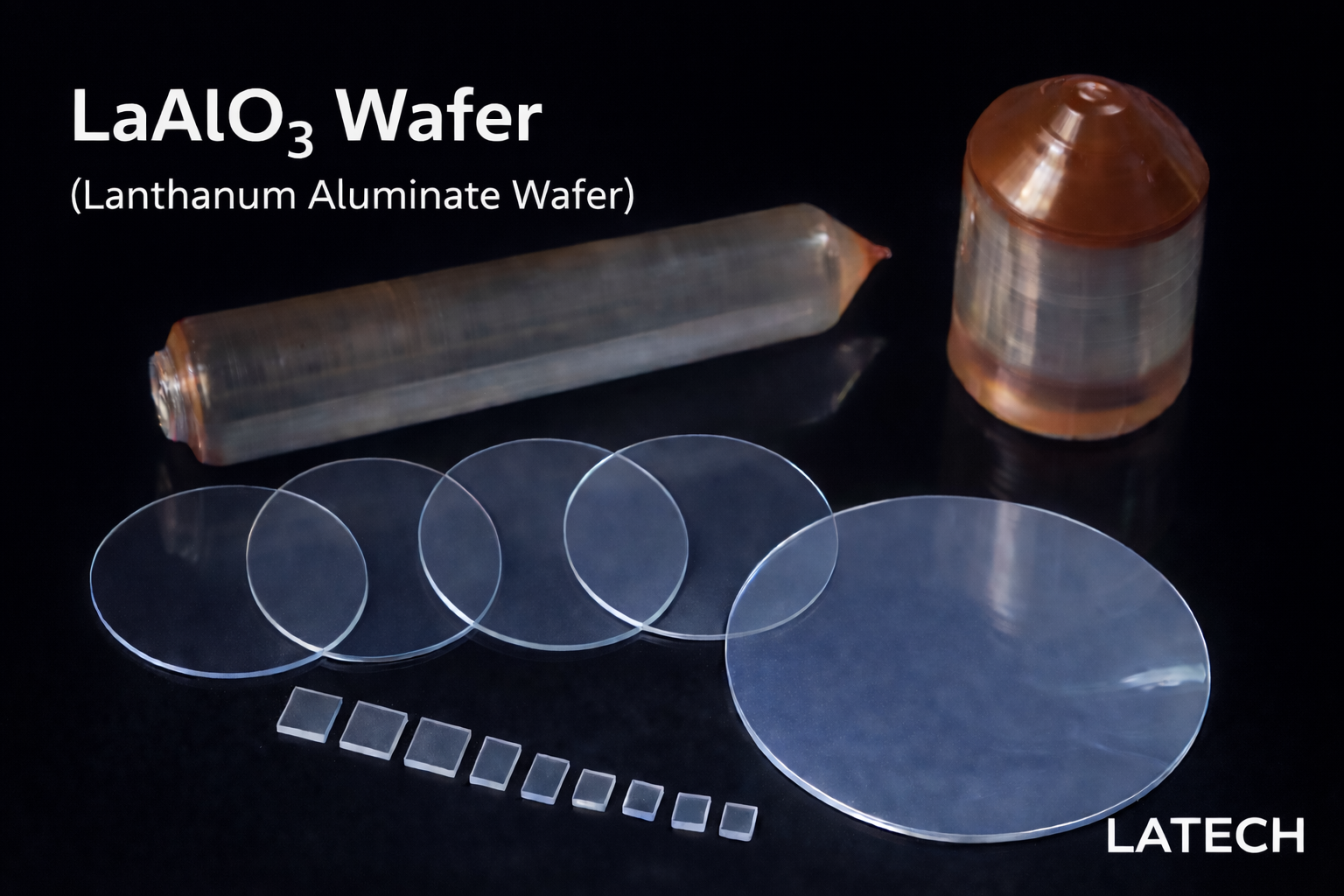
Single crystal LaAlO₃ substrate for epitaxial growth of oxide thin films and superconducting materials
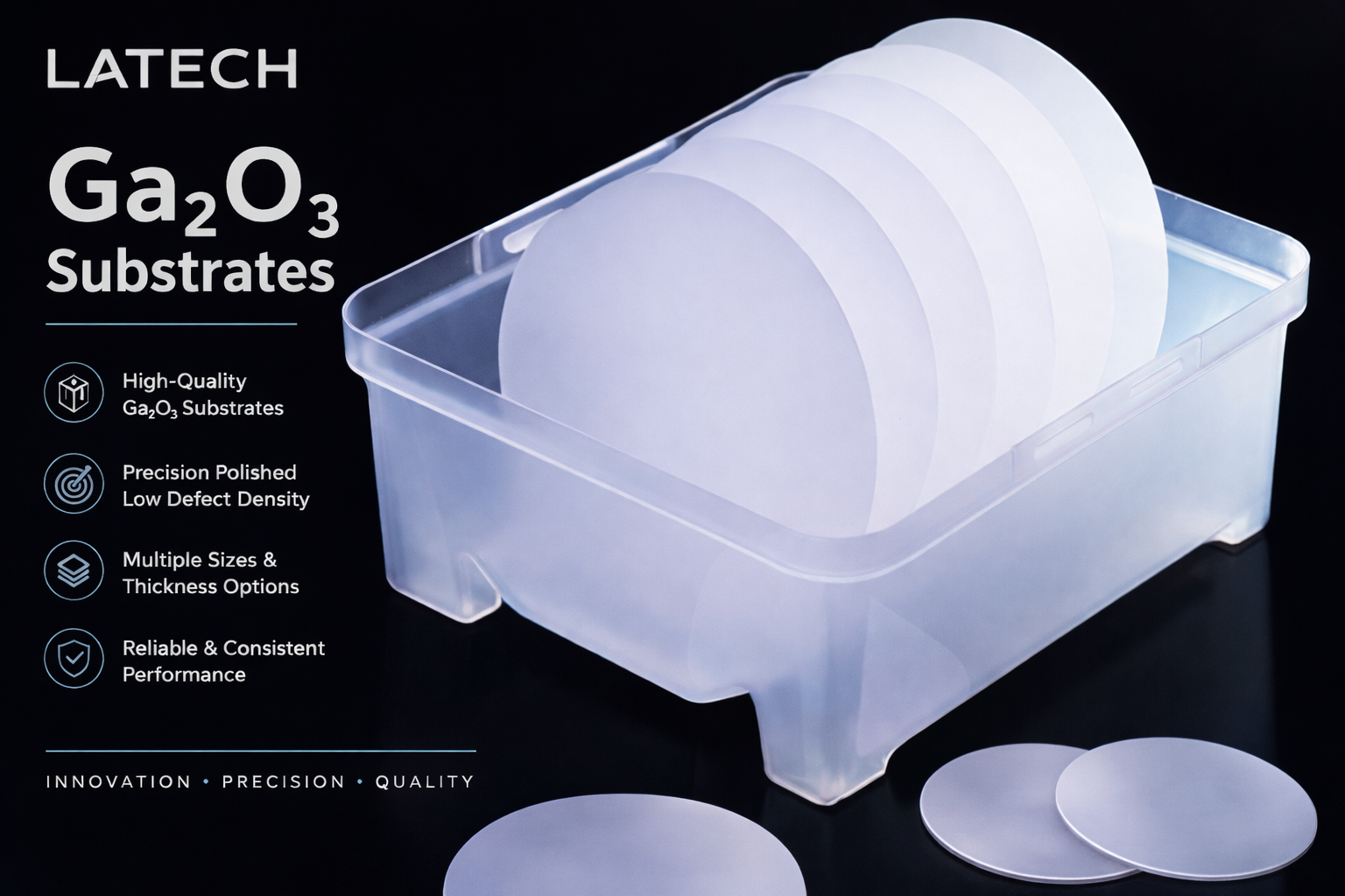
Epi-ready single crystal β-Ga₂O₃ substrate for power electronics and UV applications
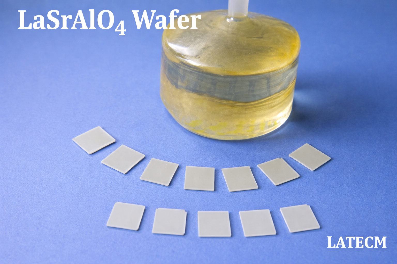
High-quality perovskite-related substrate for superconducting thin films and oxide epitaxy
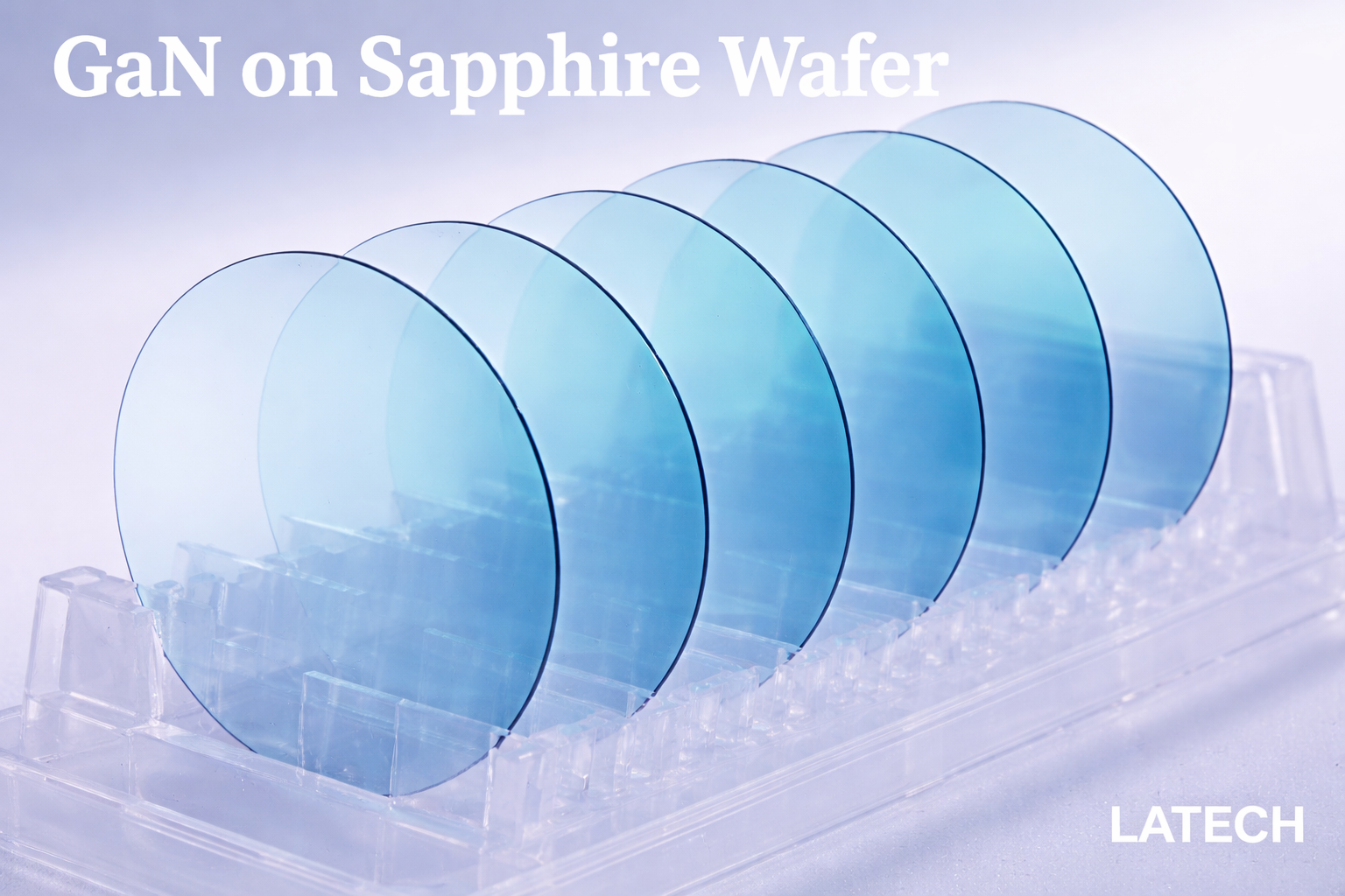
Wide bandgap semiconductor wafer for LED, RF, and high-power electronic applications

Tell us about your needs.
We will recommend the best fits for you.