
CdTe Wafer (Cadmium Telluride Wafer)
High-performance CdTe wafers for photovoltaic, infrared, and radiation detection applications.
Description
🔷 Overview
Cadmium Telluride (CdTe) wafers are II–VI compound semiconductor substrates widely used in photovoltaic, optoelectronic, and radiation detection applications.
CdTe features a near-ideal direct bandgap (~1.5 eV) that closely matches the solar spectrum, enabling highly efficient energy conversion. It also exhibits a very high absorption coefficient (>10⁴–10⁵ cm⁻¹), allowing efficient light absorption even with thin material layers.
In addition, its high atomic number and high resistivity make CdTe an excellent material for X-ray and gamma-ray detection, capable of operating at room temperature without complex cooling systems.
🔷 Key Features
- Direct bandgap (~1.5 eV) ideal for photovoltaic applications
- High absorption coefficient (>10⁴–10⁵ cm⁻¹)
- Efficient light absorption with thin material layers
- Requires significantly thinner absorber layers compared to silicon
- High atomic number for radiation detection
- Capable of room-temperature operation
- High resistivity and excellent stability
- Suitable for optoelectronic and detector applications
🔷 Specifications
|
Product: |
Single crystal Cadmium Telluride (CdTe) wafer |
|
Material property: |
Crystal structure: Cubic |
|
Lattice constant: a = 6.483 Å |
|
|
Density: 5.851 g/cm3 |
|
|
Melting Point: 1047 °C |
|
|
Thermal Conductivity: 6.3 W/K.m at 300 K |
|
|
Thermal Expansion Coefficient: 5.9 × 10⁻⁶ /K |
|
|
Transmission Range: ~0.85 µm – 25 µm (IR transparent) |
|
|
Refractive Index (n): ~2.7 at 10 µm |
|
|
Growth Method: PVT |
|
|
Conductive type
|
• Un-doped • P-type |
|
Dimension: |
• 5 × 5 × 0.5 mm • 5 × 10 × 0.5 mm • 10 × 10 × 0.5 mm • 20 × 20 × 0.5 mm • Other sizes customizable |
|
Orientation: |
• <100> ± 0.5° • <001> ± 0.5° • <110> ± 0.5° • <111> ± 0.5° |
|
Polishing: |
• Fine ground • Single side epi-polished • double side epi-polished |
|
Surface roughness: |
< 0.5 nm |
🔷 Applications
- Thin-film solar cells (photovoltaics)
- Infrared and optical devices
- X-ray and gamma-ray detectors
- Medical imaging systems
- Semiconductor and optoelectronic research
🔷 Customization Options
We support customized CdTe wafers based on your requirements:
- Diameter and thickness
- Orientation and off-angle
- Doping type and resistivity
- Surface polishing (SSP / DSP)
- Detector-grade or photovoltaic-grade material
Related Products
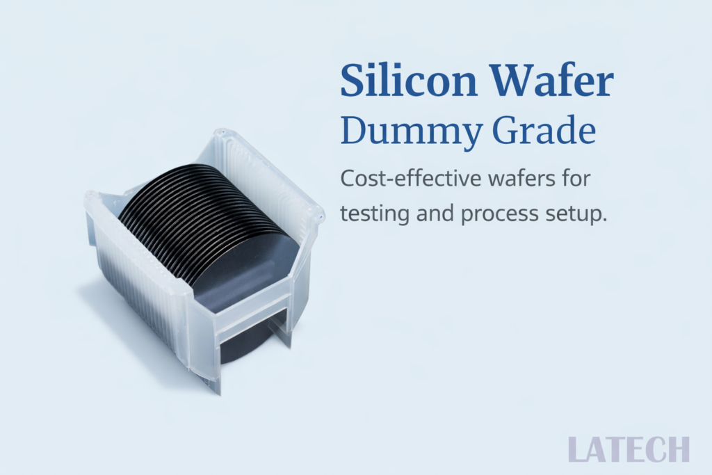
Dummy Grade Silicon Wafer
Elemental Wafer
Wafer
Cost-effective silicon wafer for process testing, equipment calibration, and non-critical applications
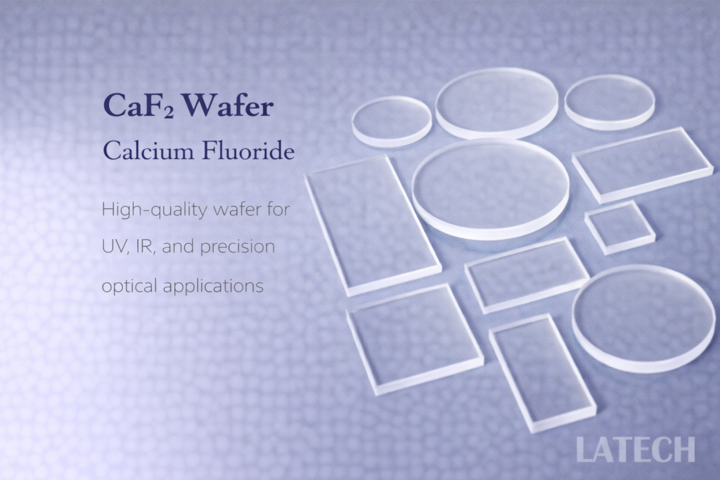
CaF₂ Wafer (Calcium Fluoride Substrate)
Binary Wafer
Wafer
High-quality CaF₂ wafers for UV, IR, and high-precision optical applications.
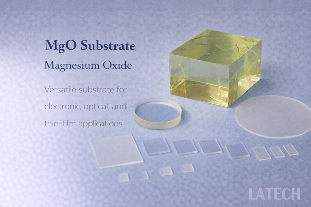
MgO Wafer (Magnesium Oxide Substrate)
Binary Wafer
Wafer
High-quality MgO wafers for superconducting, epitaxial, and thin-film applications.
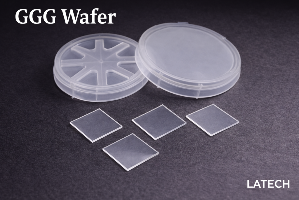
GGG Wafer (Gadolinium Gallium Garnet, Gd₃Ga₅O₁₂ Wafer)
Wafer
Ternary Wafer
High-quality garnet substrate for magnetic thin films and oxide epitaxy
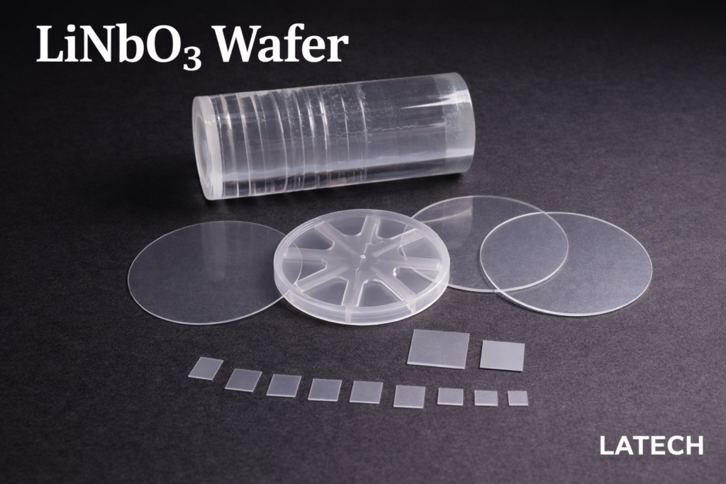
LiNbO₃ Wafer (Lithium Niobate Substrate)
Wafer
Ternary Wafer
High-performance electro-optic and piezoelectric substrate for photonics, modulators, and SAW devices