Wafer
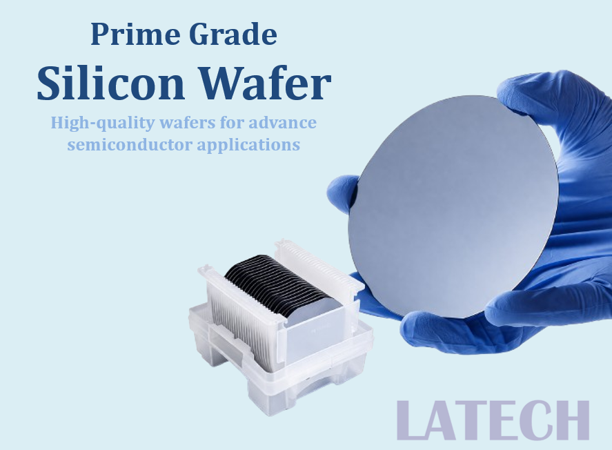
Prime Grade Silicon Wafer
High purity monocrystalline silicon substrate for semiconductor and research applications
High purity monocrystalline silicon substrate for semiconductor and research applications


Highly conductive and transparent FTO glass, now 1.1 / 2.2 / 3.3 mm thicknesses available, can cut into any sizes


Holey/lacey supporting film, with open holes for characterization without background inteference


High-quality CaF₂ wafers for UV, IR, and high-precision optical applications.

High purity quartz, up to 1100 °C, most commonly used tubes in tube furnaces

Standard cuvettes for UV-Vis spectrophotometry with two optical clear walls for accurate absorbance measurements


High-temperature stable oxide substrate for epitaxy, buffer layers, and solid oxide fuel cells


Self-closing for easier manipulation of small objects, with ultrasharp straight tips

Highest quality quartz slides, with mirror or epi-polished surfaces! Different material grades of choices

Sealed cuvette for accurate fluorescence measurements with four optical windows

Cost-effective cuvettes for routine measurements with no cleaning required

Innovative Al-doped ZnO conductive glass, easy to process, high conductivity and transparency

Laser etched, any patterns upon your request, highly transparent before and after laser etching


One of the best choices for grinding purpose, high precision beads are also available for axletree.

High purity natural graphite, customizable sizes, up to 2500 °C in inert or reducing atmosphere


Nanoscale surface topography analyses, for nanomaterials, biology samples, liquid samples, etc
Tell us about your needs.
We will recommend the best fits for you.