
GaAs Wafer (Gallium Arsenide Wafer)
High-performance GaAs wafers for RF, optoelectronic, and high-speed applications.
Description
🔷 Overview
Gallium Arsenide (GaAs) wafers are III–V compound semiconductor substrates widely used in high-frequency electronics, optoelectronics, and advanced communication systems.
GaAs features a direct bandgap (~1.4–1.43 eV), enabling efficient light emission and absorption, making it ideal for laser diodes, LEDs, and photonic devices.
Compared with silicon, GaAs offers significantly higher electron mobility (5–6× higher), allowing faster signal transmission and superior performance in RF and microwave applications.
In addition, GaAs exhibits low noise characteristics, strong radiation resistance, and excellent high-frequency performance, making it widely used in satellite communication, radar systems, and wireless networks.
🔷 Key Features
- Direct bandgap (~1.4 eV) for efficient light emission
- High electron mobility for high-speed electronics
- Excellent performance in RF and microwave applications
- Low noise characteristics for communication systems
- Strong radiation resistance for aerospace applications
- High-frequency capability for mmWave and 5G devices
- Suitable for optoelectronic and photonic applications
🔷 Specifications
|
Product: |
Single crystal GaAs wafer |
|
Material property: |
Crystal structure: Rhombohedral |
|
Lattice constant: a = 5.6534 Å, |
|
|
Melting point: 1237 °C |
|
|
Dielectric constant: 13.1 |
|
|
Dislocation Density: <5×10³ cm⁻² |
|
|
Electron mobility: 3500-3600 cm²/V·s |
|
|
Growth Method: VGF |
|
|
Conductive type/ Dopant |
• Semi-insulating / un-doped • Semi-insulating / Cr-doped • N-type / Si-doped • N-type / Fe-doped • P-type / Zn-doped |
|
Carrier concentration |
• > 5 × 10¹⁷ • > 2 × 10¹⁸ |
|
Dimension: |
• 5 × 5 × 0.5 mm • 5 × 10 × 0.5 mm • 10 × 10 × 0.5 mm • 20 × 20 × 0.5 mm • φ2″ × 0.35 mm • φ3″ × 0.5 mm • φ4″ × 0.6 mm • φ6″ × 0.65 mm • Other sizes customizable |
|
Orientation: |
• <100> ± 0.5° • <100> with 2° off toward <111> |
|
Polishing: |
• Fine ground • Single side epi-polished • double side epi-polished |
|
Surface roughness: |
< 0.5 nm |
🔷 Applications
- RF and microwave devices (amplifiers, MMICs)
- Satellite communication and radar systems
- Optical communication systems
- Laser diodes and LEDs
- High-efficiency solar cells
- Wireless communication (5G, WLAN, GPS)
- Aerospace and defense electronics
🔷 Why Choose GaAs Over Silicon
- Direct bandgap enables efficient light emission (Si cannot)
- Much higher electron mobility for faster devices
- Better performance at high frequencies (RF/mmWave)
- Lower noise for communication systems
- Strong radiation resistance for space applications
🔷 Customization Options
We support customized GaAs wafers based on your requirements:
- Diameter and thickness
- Orientation and off-angle
- Conductive type and doping
- Surface polishing (SSP / DSP)
- Epitaxial-ready wafers
Related Products
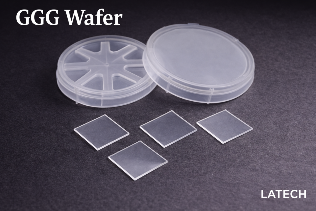
GGG Wafer (Gadolinium Gallium Garnet, Gd₃Ga₅O₁₂ Wafer)
Wafer
Ternary Wafer
High-quality garnet substrate for magnetic thin films and oxide epitaxy

LiAlO₂ Wafer (Lithium Aluminate Substrate)
Wafer
Ternary Wafer
High-performance substrate for GaN epitaxy, superconducting films, and microwave applications
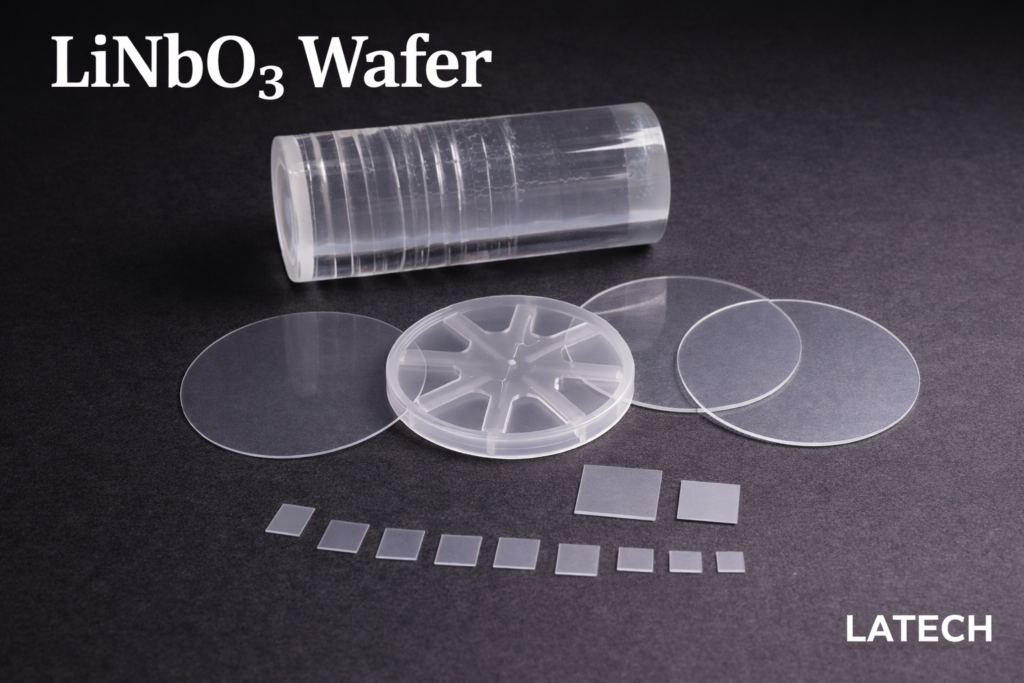
LiNbO₃ Wafer (Lithium Niobate Substrate)
Wafer
Ternary Wafer
High-performance electro-optic and piezoelectric substrate for photonics, modulators, and SAW devices

TiO₂ Wafer (Titanium Dioxide Substrate)
Binary Wafer
Wafer
High-quality TiO₂ substrates for optical, photonic, and thin-film applications.
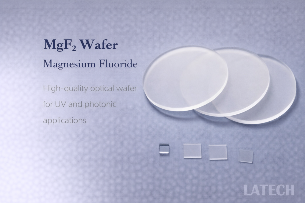
MgF₂ Wafer (Magnesium Fluoride Substrate)
Binary Wafer
Wafer
High-quality MgF₂ wafers for UV, optical, and photonic applications.