Wafer
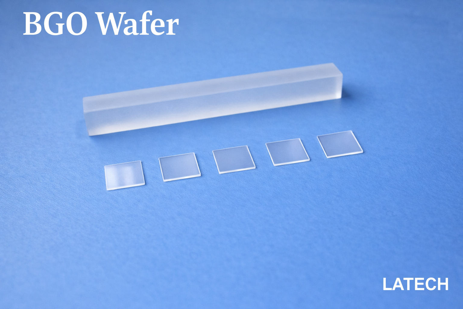
BGO Wafer (Bismuth Germanate, Bi₄Ge₃O₁₂ Wafer)
High-density scintillation crystal substrate for radiation detection and optoelectronic applications
High-density scintillation crystal substrate for radiation detection and optoelectronic applications

High birefringence optical crystal substrate for polarization and photonic applications
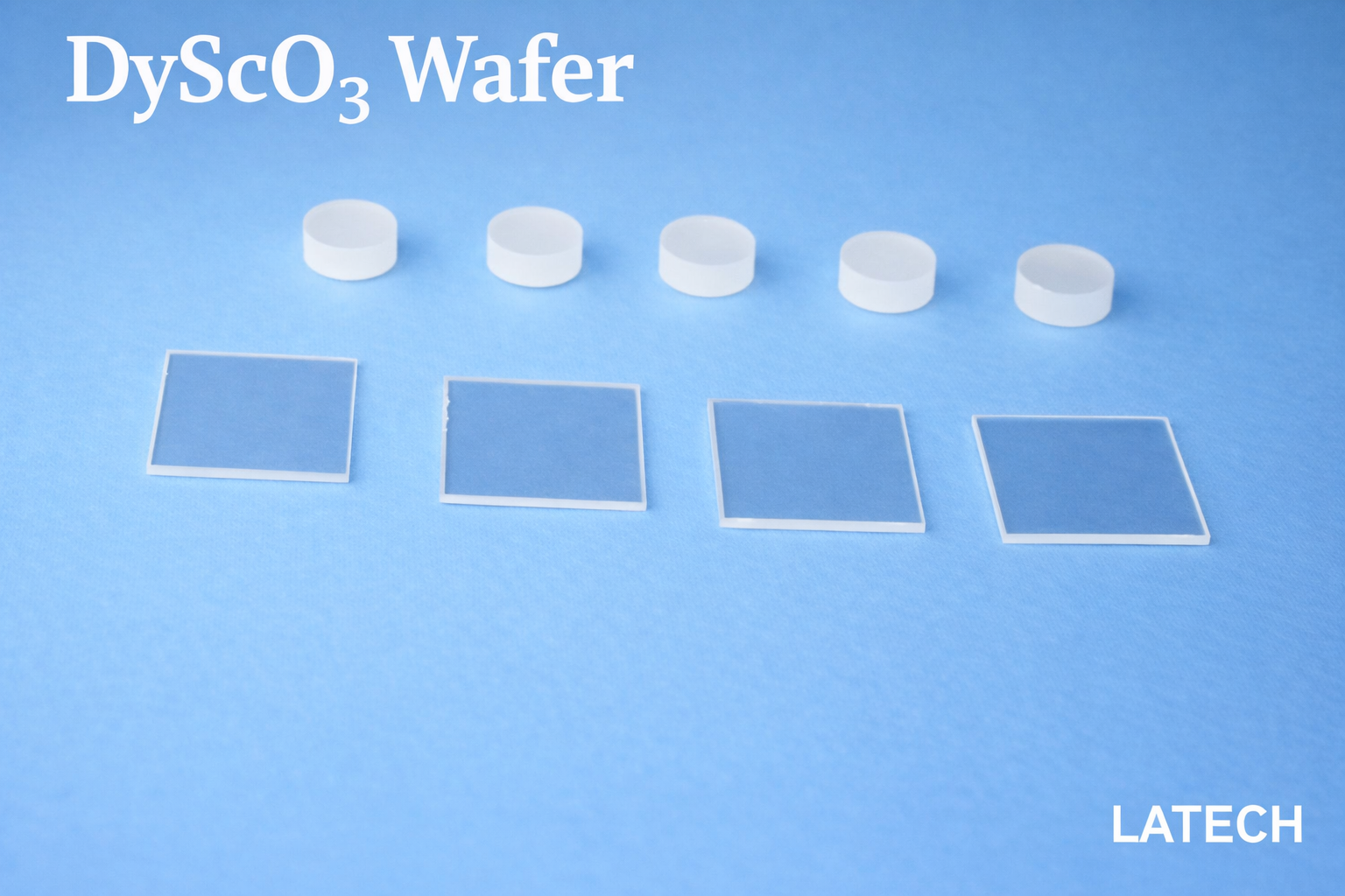
High-quality rare-earth scandate substrate for oxide epitaxy and strain engineering

High-quality rare-earth scandate substrate for advanced oxide epitaxy and strain engineering

High-quality garnet substrate for magnetic thin films and oxide epitaxy

High-quality cubic perovskite substrate for oxide electronics and epitaxial growth
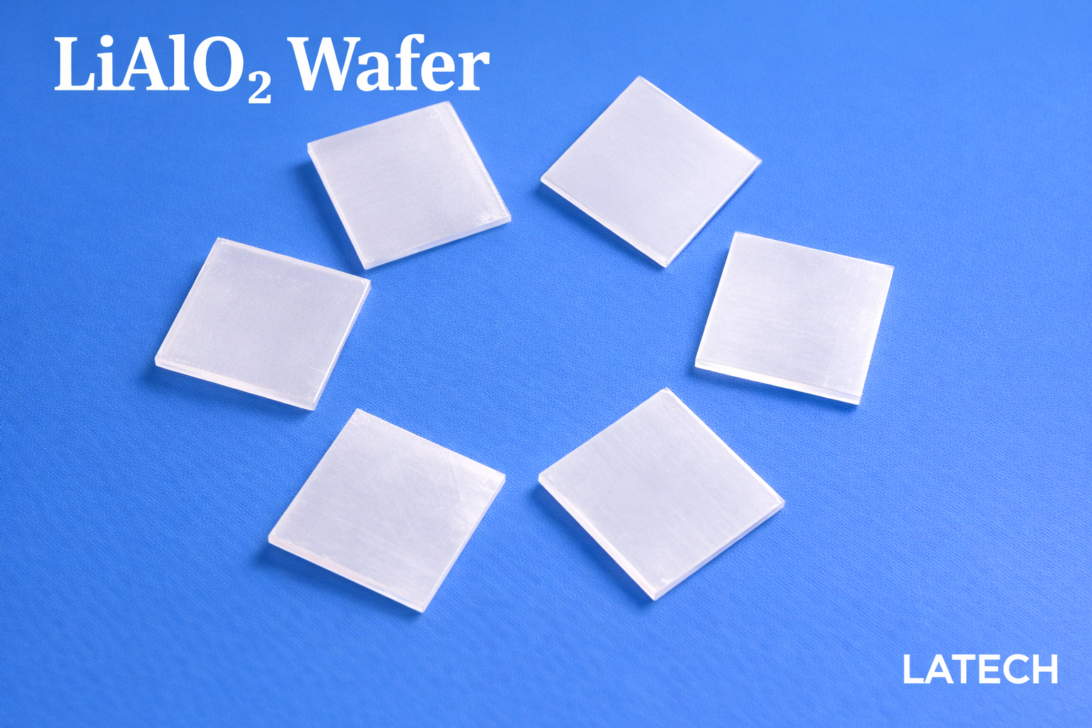
High-performance substrate for GaN epitaxy, superconducting films, and microwave applications

High-performance electro-optic and piezoelectric substrate for photonics, modulators, and SAW devices
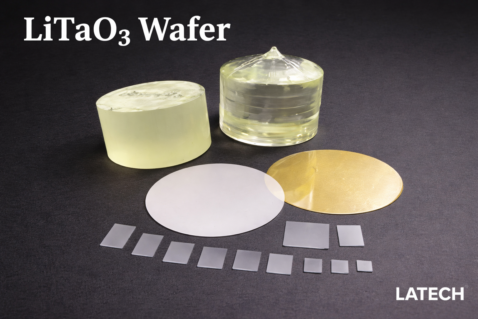
High-performance piezoelectric and electro-optic substrate for SAW devices, sensors, and photonic applications

High-performance insulating spinel substrate for microwave devices, GaN epitaxy, and advanced thin film applications

High-quality perovskite oxide substrate for superconducting, magnetic, and epitaxial thin film applications
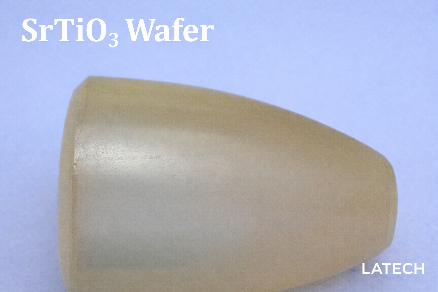
High-quality insulating perovskite oxide substrate for epitaxial growth and advanced oxide thin film applications
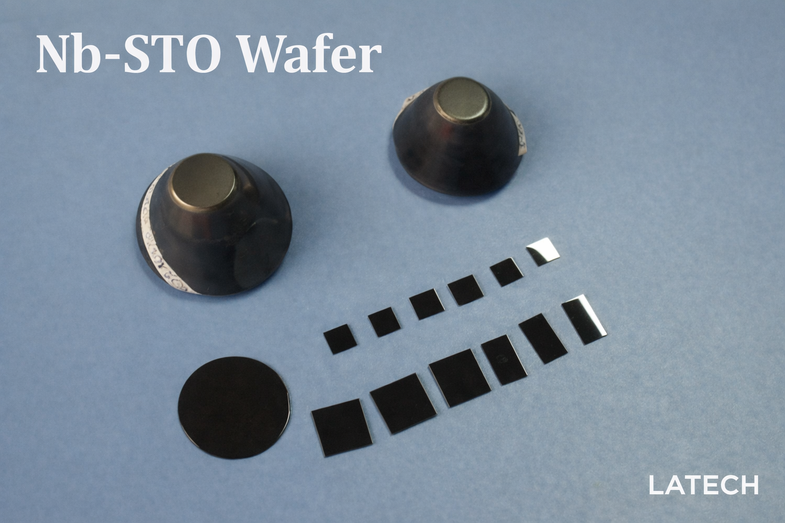
Conductive perovskite oxide substrate for epitaxial growth, oxide electronics, and advanced functional materials

Semiconducting perovskite oxide substrate for oxide electronics and advanced thin film applications
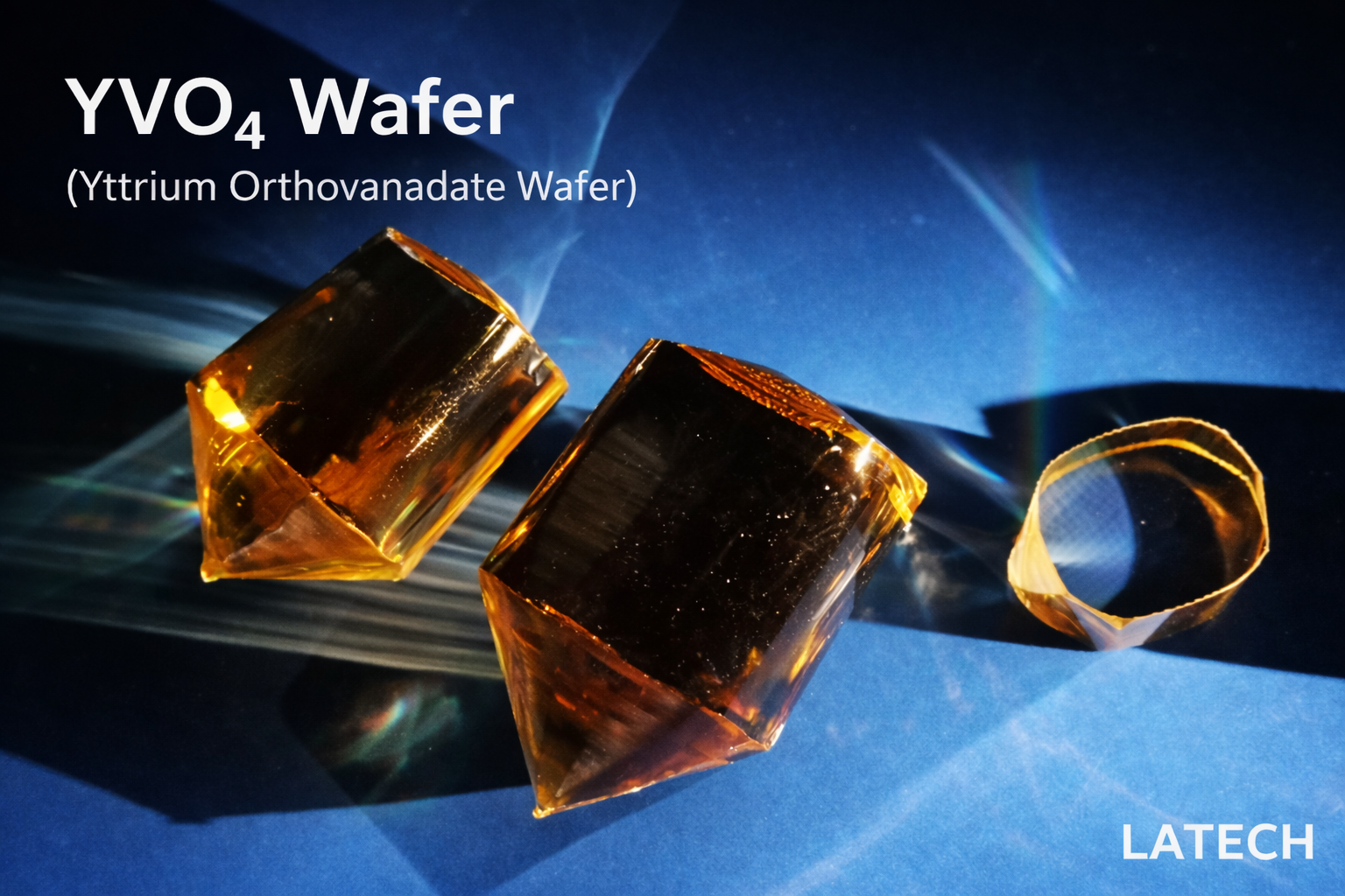
High-quality single crystal YVO₄ substrate for optical and photonic applications
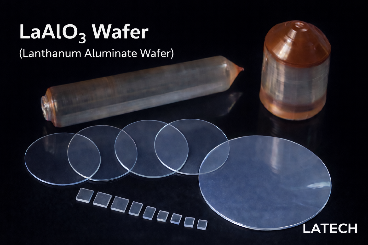
Single crystal LaAlO₃ substrate for epitaxial growth of oxide thin films and superconducting materials
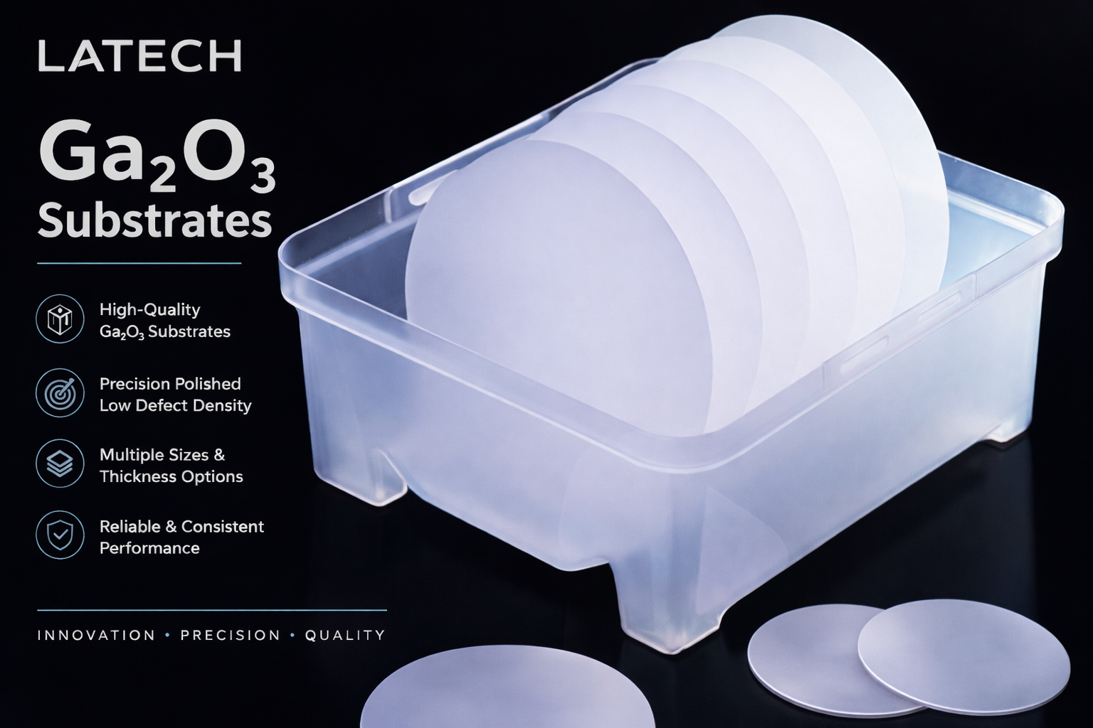
Epi-ready single crystal β-Ga₂O₃ substrate for power electronics and UV applications
Tell us about your needs.
We will recommend the best fits for you.