
GaN Wafer (Gallium Nitride Wafer)
High-performance GaN wafers for power electronics, RF, and optoelectronic applications.
Description
🔷 Overview
Gallium Nitride (GaN) wafers are wide bandgap III–V semiconductor substrates widely used in power electronics, high-frequency devices, and optoelectronics.
With a wide bandgap of approximately 3.4 eV, GaN enables devices to operate at higher voltages, higher temperatures, and higher frequencies compared to conventional materials such as silicon and GaAs.
GaN also offers excellent thermal stability and high electron velocity, making it ideal for high-efficiency power devices and RF applications such as HEMTs and microwave amplifiers.
GaN wafers are available in various forms, including freestanding GaN substrates, GaN-on-sapphire, GaN-on-Si, and GaN-on-SiC, providing flexibility for different device architectures and cost-performance requirements.
🔷 Key Features
- Wide bandgap (~3.4 eV) for high-power operation
- High breakdown voltage and high-temperature stability
- High electron mobility and velocity for RF applications
- Excellent thermal conductivity and reliability
- Suitable for high-frequency and high-efficiency devices
- Radiation-resistant material for aerospace applications
- Available in multiple substrate configurations
🔷 Specifications
|
Product: |
Single crystal GaN wafer |
|
Material property: |
Crystal structure: Hexagonal |
|
Lattice constant: a = 3.186 Å, c = 5.186 Å |
|
|
Density: 6.15 g/cm3 |
|
|
Dislocation density: (5-9) x 10^5 cm^-2 |
|
|
Dielectric constant: 8.9 |
|
|
Growth Method: HVPE |
|
|
Dimension: |
• 5 × 5 mm • 5 × 10 mm • 10 × 10 mm • Dia 2″ mm • Dia 3″ mm • Other sizes customizable |
|
Thickness: |
350 ± 20 um; 500 ± 20 um |
|
Orientation: |
• C-axis (0001) ± 1.0° • M-axis (10-10) ± 1.0° |
|
Dopant / Conductive |
• Undoped / N-type (Resistivity: < 0.5 ohm.cm) • Semi-insulating / Fe-doped (Resistivity: > 10E6 ohm.cm) • Si-doped / N-type (Resistivity: < 0.05 ohm.cm) |
|
Polishing: |
• Fine ground • Single side epi-polished • double side epi-polished |
|
Surface roughness: |
< 0.5 nm |
🔷 Applications
- Power electronics (power devices, converters)
- RF and microwave devices (HEMTs, amplifiers)
- LED and laser diodes (blue, green, UV)
- 5G and high-frequency communication systems
- Electric vehicles and energy systems
- Aerospace and satellite electronics
🔷 Why Choose GaN Over Silicon
- Higher breakdown voltage for power devices
- Better efficiency in high-frequency applications
- Operation at higher temperatures
- Lower energy loss in power conversion
- Smaller device size with higher performance
🔷 Customization Options
We support customized GaN wafers based on your requirements:
- Substrate type (GaN / Sapphire / Si / SiC)
- Diameter and thickness
- Doping type
- Surface polishing
- Epitaxial-ready wafers
Related Products

TiO₂ Wafer (Titanium Dioxide Substrate)
Binary Wafer
Wafer
High-quality TiO₂ substrates for optical, photonic, and thin-film applications.

KTaO₃ Wafer (Potassium Tantalate Wafer)
Wafer
Ternary Wafer
High-quality cubic perovskite substrate for oxide electronics and epitaxial growth

LiAlO₂ Wafer (Lithium Aluminate Substrate)
Wafer
Ternary Wafer
High-performance substrate for GaN epitaxy, superconducting films, and microwave applications
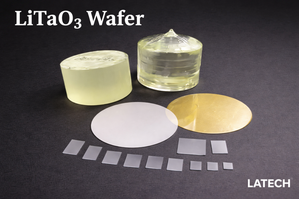
LiTaO₃ Wafer (Lithium Tantalate Substrate)
Wafer
Ternary Wafer
High-performance piezoelectric and electro-optic substrate for SAW devices, sensors, and photonic applications
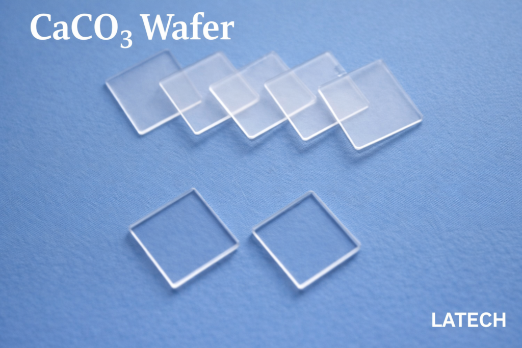
CaCO₃ Wafer (Calcium Carbonate Wafer)
Wafer
Ternary Wafer
High birefringence optical crystal substrate for polarization and photonic applications