
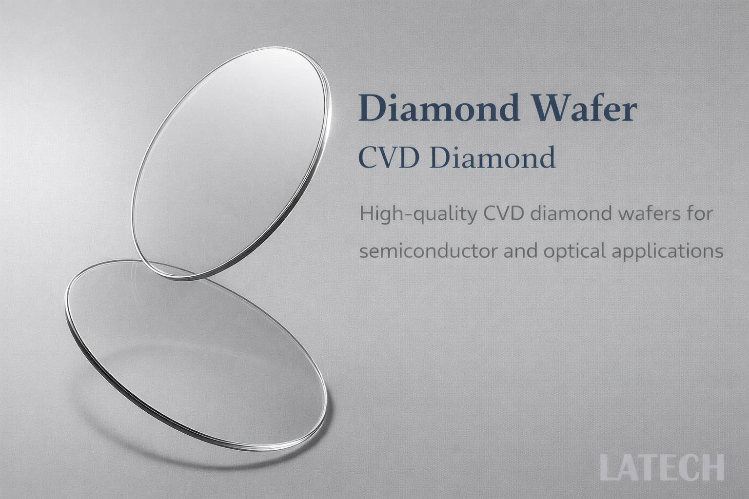
Diamond Wafer (CVD Diamond Wafer)
High-performance diamond wafers for optical, thermal, and semiconductor applications.
Description
🔷 Overview
Diamond wafers are advanced materials known for their exceptional thermal conductivity, optical transparency, and mechanical hardness.
Our single-crystal CVD diamond wafers are produced using MPCVD technology, ensuring high purity, excellent surface quality, and stable performance for demanding applications.
They are widely used in high-power electronics, optics, and next-generation semiconductor devices.
🔷 Product Types
We offer different types of diamond wafers to meet various application requirements:
- Microelectronics Grade – for semiconductor devices and epitaxy applications
- Thermal Grade – for heat spreaders and thermal management
- Optical Grade – for optical windows, laser systems, and photonics
🔷 Key Features
- Exceptional thermal conductivity (>1000 W/m·K)
- Excellent optical transparency (UV to IR range)
- High electron and hole mobility
- Ultra-low impurity levels (ppb level)
- Outstanding mechanical hardness and durability
- Suitable for high-power and high-frequency applications
🔷 Specifications
|
Product |
Single crystal MPCVE diamond wafer |
|
Material property |
Refractive Index <590nm>: 2.4 |
|
Electron Mobility (cm2/VS): 4500 |
|
|
Hole Mobility (cm2/VS): 3800 |
|
|
Nitrogen Content (by EPR): < 5ppb |
|
|
Boron Content (by EPR): < 1 ppb |
|
|
Growth Method |
• MPCVD |
|
Dimension: |
• 5 × 5 mm • 10 × 5 mm • 10 × 10 mm • 20 × 20 mm • Other sizes customizable |
|
Thickness: |
• 0.2 mm ± 25 μm • 0.5 mm ± 25 μm • 1.0 mm ± 25 μm • Other sizes customizable |
|
Orientation: |
• <100> ± 0.5° • other off-angle |
|
Polishing: |
• Fine ground • Single side epi-polished • double side epi-polished |
|
Surface roughness |
< 0.5 nm |
🔷 Applications
- High-power electronic devices
- Thermal management substrates
- Optical windows and laser systems
- Quantum and advanced semiconductor research
- MEMS and sensor applications
🔷 Customization Options
We support customized diamond wafers based on your requirements:
- Size and thickness
- Orientation and off-angle
- Surface polishing (SSP / DSP)
- Optical-grade finishing
- Special application requirements
Related Products

SiO₂ Coated Silicon Wafers (Thermal Oxide Wafers)
Elemental Wafer
Wafer
High-quality silicon wafers with precisely controlled oxide layers for semiconductor and microfabrication applications.
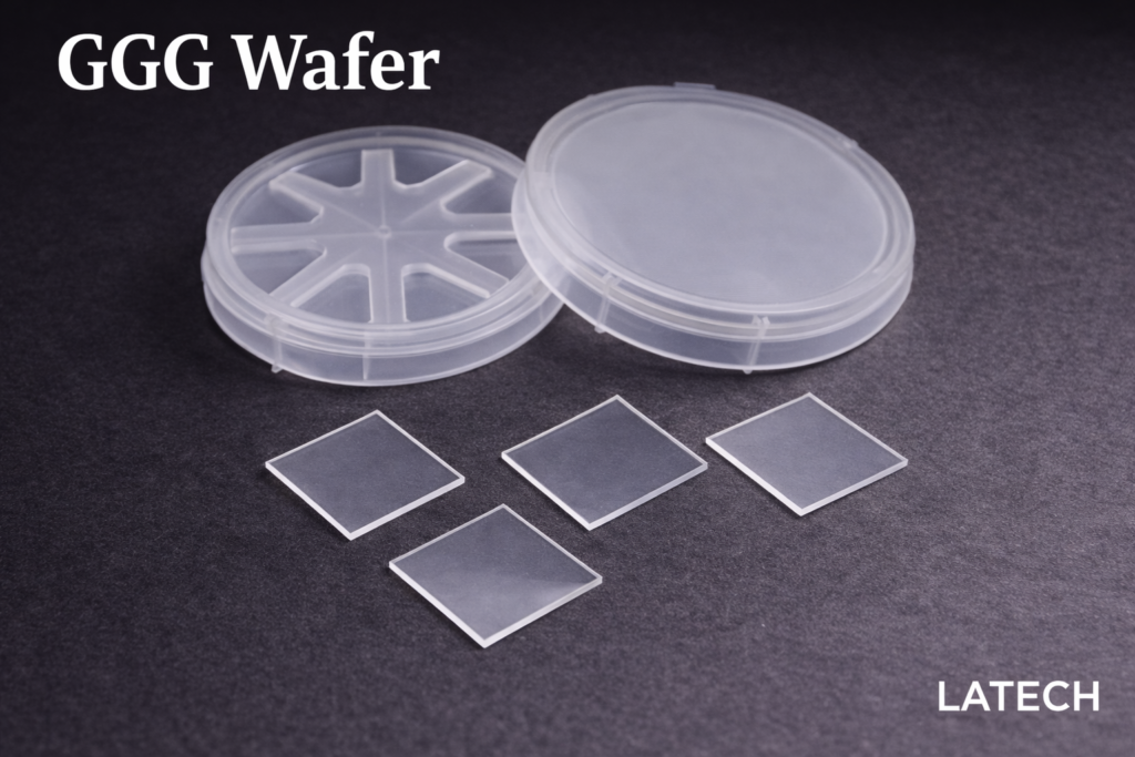
GGG Wafer (Gadolinium Gallium Garnet, Gd₃Ga₅O₁₂ Wafer)
Ternary Wafer
Wafer
High-quality garnet substrate for magnetic thin films and oxide epitaxy

LiAlO₂ Wafer (Lithium Aluminate Substrate)
Wafer
Ternary Wafer
High-performance substrate for GaN epitaxy, superconducting films, and microwave applications
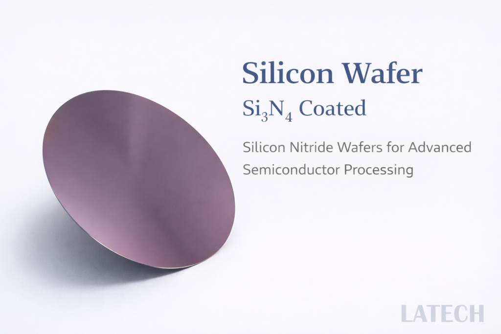
Si₃N₄ Coated Silicon Wafers (Silicon Nitride Wafers)
Elemental Wafer
Wafer
High-performance silicon wafers with silicon nitride coatings for advanced semiconductor and MEMS applications.

TiO₂ Wafer (Titanium Dioxide Substrate)
Binary Wafer
Wafer
High-quality TiO₂ substrates for optical, photonic, and thin-film applications.