
Ga₂O₃ Wafer (Beta Gallium Oxide Wafer)
Epi-ready single crystal β-Ga₂O₃ substrate for power electronics and UV applications
Description
🔷 Overview
Ga₂O₃ wafer is a single crystal beta-phase gallium oxide substrate with an ultra-wide bandgap (~4.8–4.9 eV), suitable for high-voltage devices, UV photodetectors, and epitaxial growth research.
LATECH provides high-quality β-Ga₂O₃ substrates with multiple doping options, orientations, and surface finishes for both R&D and advanced applications.
🔷 Key Features
- Ultra-wide bandgap semiconductor (~4.8–4.9 eV)
- Available in undoped, Sn-doped (n-type), and Fe-doped (semi-insulating) grades
- Common orientations: (201), (010)
- Epi-ready polished surface available
- Low surface roughness (Ra < 0.5 nm)
- Custom sizes and specifications available
🔷 Specifications
|
Product: |
Single crystal Gallium oxide (Ga2O3) wafer |
|
Material property: |
Crystal structure: Monoclinic |
|
Lattice constant: a = 12.23 Å, b = 3.04 Å, c = 5.80 Å; ß=103.7° |
|
|
Density: 5.95 g/cm3 |
|
|
Melting point: 1725 °C |
|
|
Bandgap: 4.8-4.9 eV |
|
|
Mobility: 100-200 cm2/v.s |
|
|
Growth method: CZ |
|
|
Dopant |
• Sn / N-type • Un-doped / N-type • Fe / Insulation |
|
Dimension: |
• 5 × 5 × 0.5 mm • 5 × 10 × 0.5 mm • 10 × 10 × 0.5 mm • 20 × 20 × 0.5 mm • Other sizes customizable |
|
Orientation: |
• <201> ± 0.5° • <010> ± 0.5° |
|
Polishing: |
• Fine ground • Single side epi-polished • double side epi-polished |
|
Surface roughness: |
< 0.5 nm |
🔷 Applications
- Power electronics
- UV photodetectors
- Epitaxial growth
- Semiconductor R&D
🔷 Customization
Custom specifications are available upon request:
- Size & thickness
- Orientation & off-cut
- Surface polishing
- Doping type
Related Products
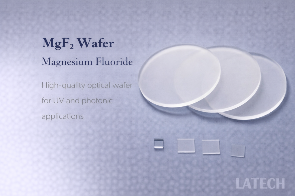
MgF₂ Wafer (Magnesium Fluoride Substrate)
Binary Wafer
Wafer
High-quality MgF₂ wafers for UV, optical, and photonic applications.
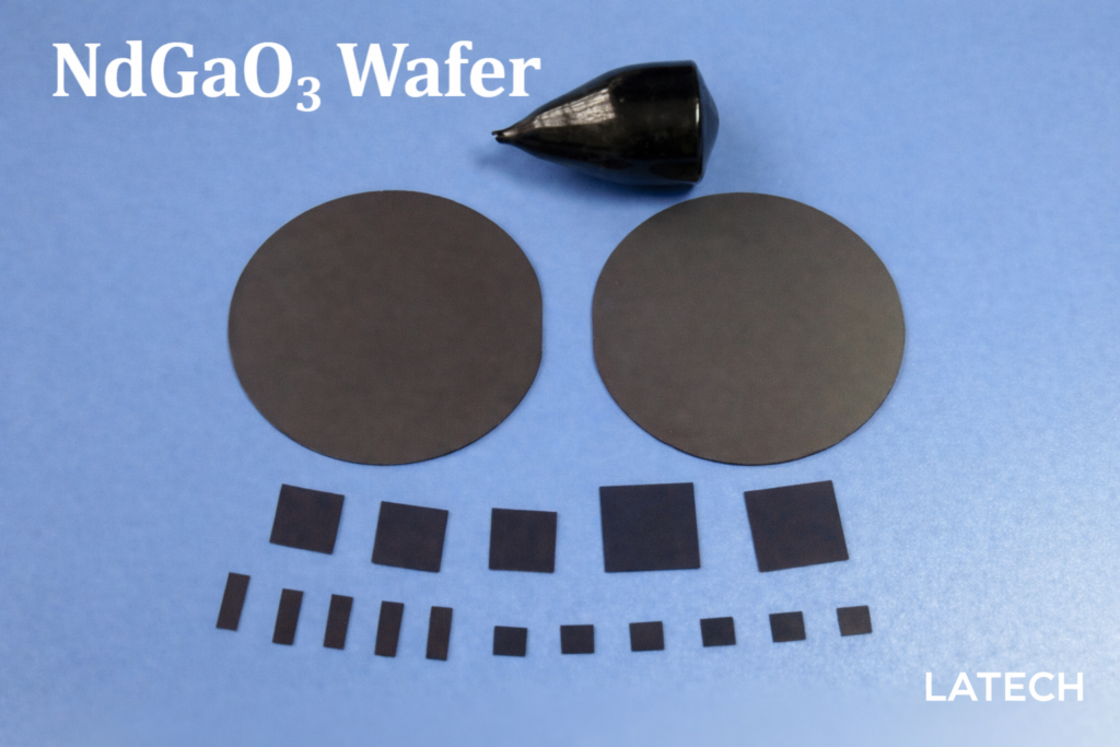
NdGaO₃ Wafer (Neodymium Gallate Substrate)
Wafer
Ternary Wafer
High-quality perovskite oxide substrate for superconducting, magnetic, and epitaxial thin film applications

KTaO₃ Wafer (Potassium Tantalate Wafer)
Ternary Wafer
Wafer
High-quality cubic perovskite substrate for oxide electronics and epitaxial growth
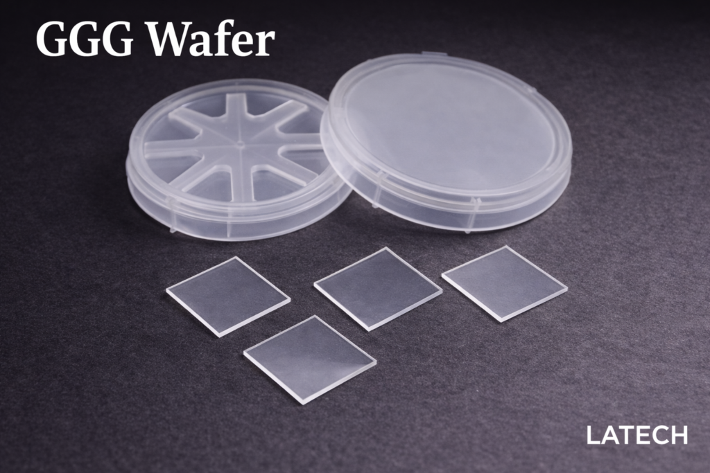
GGG Wafer (Gadolinium Gallium Garnet, Gd₃Ga₅O₁₂ Wafer)
Wafer
Ternary Wafer
High-quality garnet substrate for magnetic thin films and oxide epitaxy
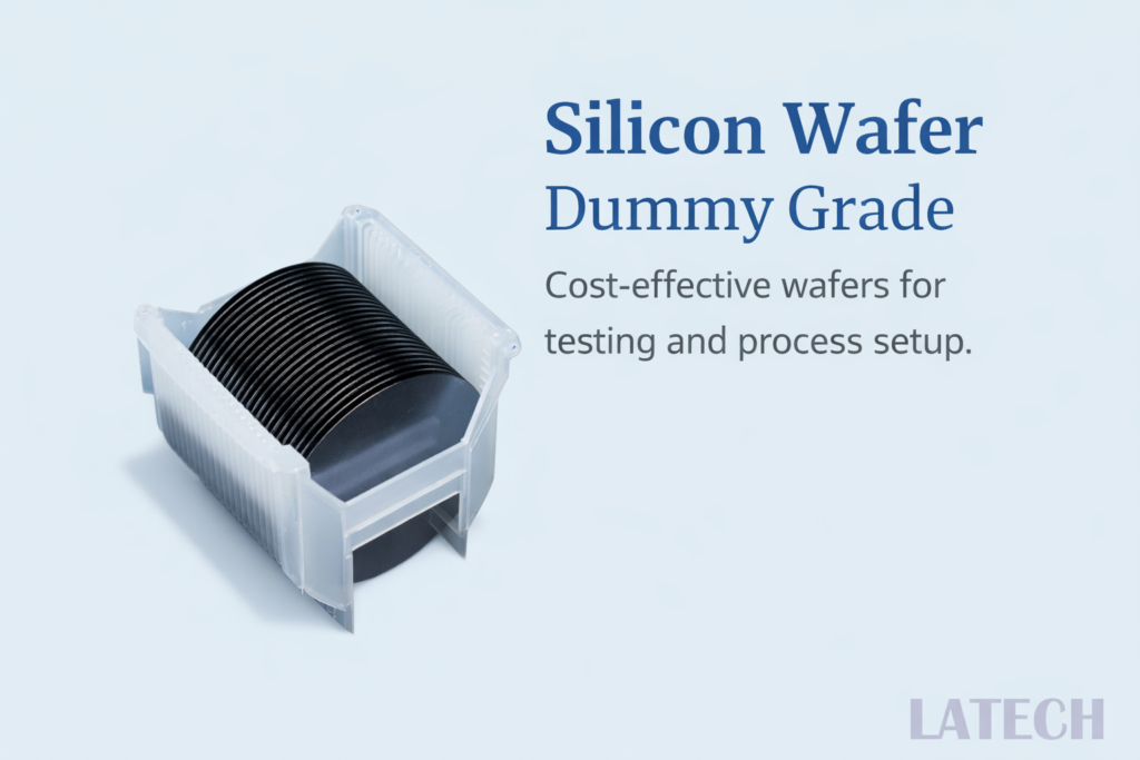
Dummy Grade Silicon Wafer
Elemental Wafer
Wafer
Cost-effective silicon wafer for process testing, equipment calibration, and non-critical applications