
Nb: SrTiO₃ Wafer (Niobium-doped Strontium Titanate Wafer)
Conductive perovskite oxide substrate for epitaxial growth, oxide electronics, and advanced functional materials
Description
🔷 Overview
Nb-doped SrTiO₃ (Nb: STO) wafer is a conductive perovskite oxide substrate widely used for epitaxial growth of complex oxide thin films and advanced electronic materials.
By introducing niobium (Nb) as a dopant, SrTiO₃ becomes electrically conductive, making it an ideal substrate for applications that require a built-in bottom electrode. Nb: STO wafers are commonly used in oxide electronics, superconducting films, ferroelectric devices, and resistive switching studies.
With excellent lattice matching to many perovskite materials and stable crystal structure, Nb: STO is a preferred choice for PLD, MBE, and sputtering deposition processes in both research and industrial applications.
🔷 Key Features
- Nb-doped SrTiO₃ provides high electrical conductivity
- Excellent lattice match for perovskite oxide thin film growth
- Stable cubic crystal structure for reliable epitaxy
- Suitable for PLD, MBE, sputtering deposition
- Good thermal and chemical stability
- Ideal for oxide electronics and superconducting research
🔷 Specifications
| Product: | Nb-Doped SrTiO3 (Nb-STO) wafer | ||||
| Appearance: |
Black Color |
||||
| Dimension: |
• 1” × 0.5 mm • 5 × 5 × 0.5 mm • 10 × 10 × 0.5 mm • 20 × 20 × 0.5 mm • Other sizes customizable |
||||
| Orientation: | <100> / <110> / <111> | ||||
| Polishing: | As cut / single side / double side epi-polished | ||||
| Surface roughness: | < 1 nm | ||||
| Physical Properties: | Nb Concentration: | 0.1 wt% | 0.4 wt% | 0.7 wt% | 1 wt% |
| Resistivity: | 0.08 ohm·cm | 0.05 ohm·cm | 0.007 ohm·cm | 0.0035 ohm·cm | |
| Mobility: | 6.5 cm2/Vs | 8.5 cm2/Vs | 8.5 cm2/Vs | 9 cm2/Vs | |
🔷 Applications
- Oxide thin film epitaxy (PLD / MBE / sputtering)
- High-temperature superconductors (HTS)
- Ferroelectric and dielectric materials
- Transparent conductive substrates
- Resistive switching / memristor devices
- Spintronics and oxide electronics
🔷 Why Choose Nb: SrTiO₃
- Conductive substrate → eliminates need for bottom electrode
- Excellent lattice matching with perovskite oxides
- Widely used in academic & advanced materials research
- Stable and reproducible performance
🔷 Customization Options
- Doping concentration (Nb level)
- Orientation & off-cut
- Thickness & size
- Surface finish (SSP / DSP / Epi-ready)
- Research-grade / device-grade
Related Products

TiO₂ Wafer (Titanium Dioxide Substrate)
Binary Wafer
Wafer
High-quality TiO₂ substrates for optical, photonic, and thin-film applications.
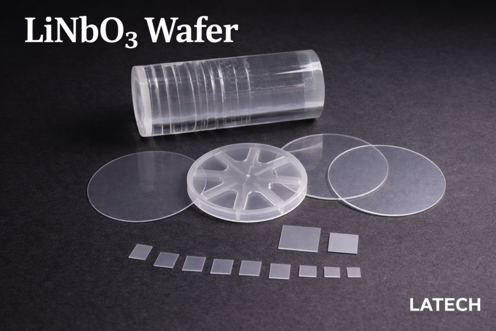
LiNbO₃ Wafer (Lithium Niobate Substrate)
Wafer
Ternary Wafer
High-performance electro-optic and piezoelectric substrate for photonics, modulators, and SAW devices
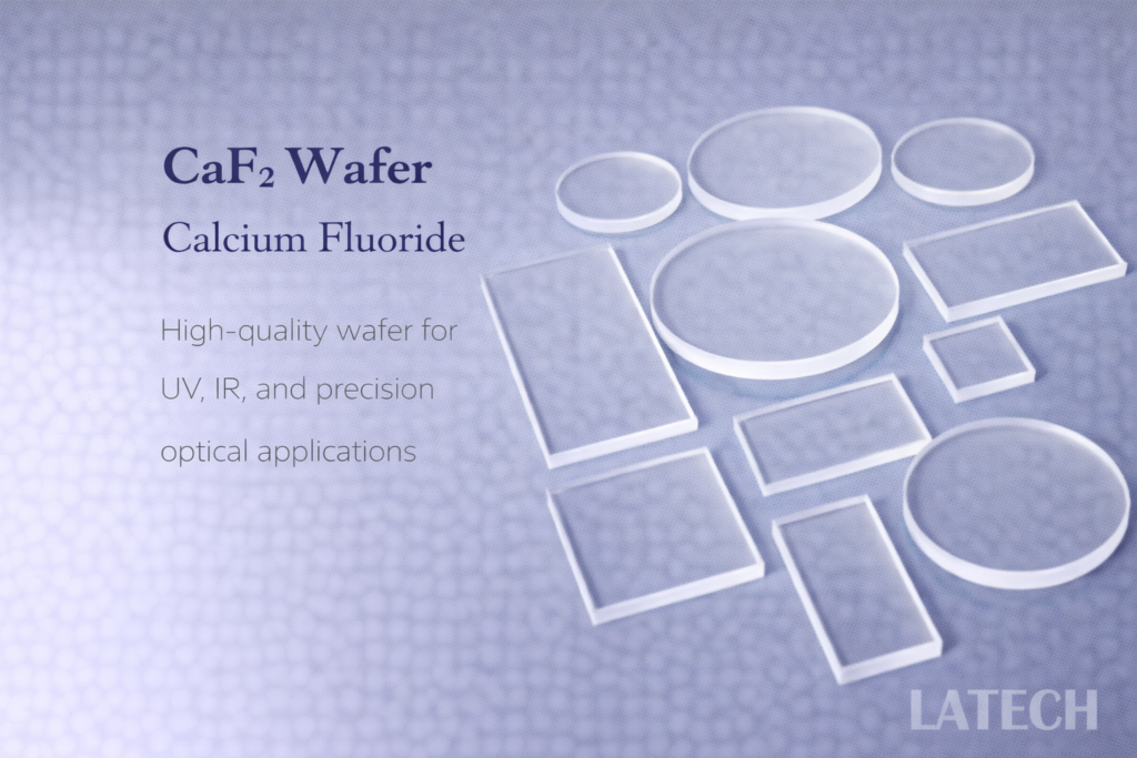
CaF₂ Wafer (Calcium Fluoride Substrate)
Binary Wafer
Wafer
High-quality CaF₂ wafers for UV, IR, and high-precision optical applications.

DyScO₃ Wafer (Dysprosium Scandate Wafer)
Ternary Wafer
Wafer
High-quality rare-earth scandate substrate for oxide epitaxy and strain engineering
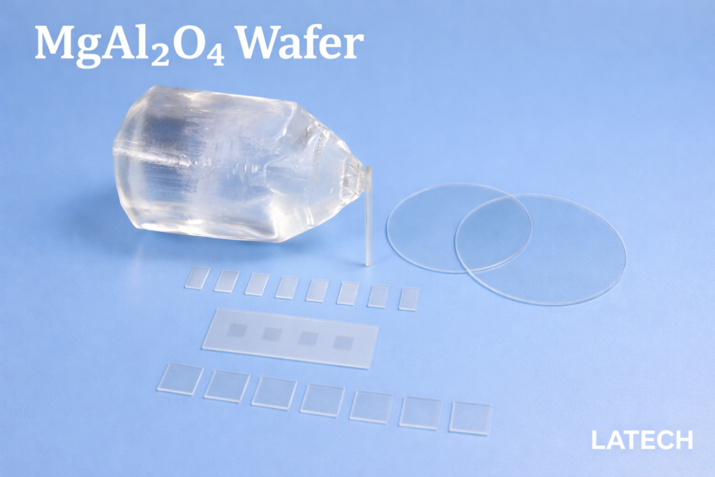
MgAl₂O₄ Wafer (Magnesium Aluminate Spinel Substrate)
Wafer
Ternary Wafer
High-performance insulating spinel substrate for microwave devices, GaN epitaxy, and advanced thin film applications