
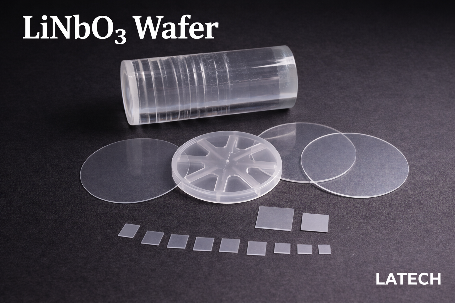
LiNbO₃ Wafer (Lithium Niobate Substrate)
High-performance electro-optic and piezoelectric substrate for photonics, modulators, and SAW devices
Description
🔷 Overview
Lithium Niobate (LiNbO₃) wafer is a multifunctional single crystal substrate widely used in photonics, telecommunications, and acoustic devices.
It exhibits outstanding electro-optic, piezoelectric, and nonlinear optical properties, making it one of the most important materials for optical modulators, waveguides, and SAW devices.
With high refractive index (>2.3) and excellent optical transmission, LiNbO₃ is ideal for integrated optics and high-speed optical communication systems.
🔷 Key Features
- Excellent electro-optic (Pockels effect) performance
- Strong piezoelectric and acousto-optic properties
- High nonlinear optical coefficient (frequency doubling, OPO)
- Wide optical transmission (~350 nm – 5.2 µm)
- High refractive index (>2.3)
- Stable crystal structure and good mechanical strength
🔷 Specifications
|
Material |
3″ 4″ 6″ 8″ lithium niobate (LiNbO3) wafer for both Saw/Optical grade |
|
Orientation |
X/Z/Y41°/Y64°/Y128°/YZ/YX or Customized |
|
Surface finish |
single or double sides polish (DLP/SLP/ SSP/DSP all available ) |
|
Thickness |
0.18/0.25/0.35/0.50/1.00 + mm |
|
TTV |
< 1~5µm |
|
BOW |
± (25µm ~40um ) |
|
Warp |
<= 35µm |
|
LTV (5mmx5mm) |
<1.5 um |
|
PLTV(<0.5um) |
≥98% (5mm x 5mm) with 2mm edge excluded |
|
Curie Temp |
1142°C±3°C |
|
Edge |
Comply with SEMI M1.2@with GC800#. regular at C typed |
|
Orientation flats |
available, per request |
|
Doped with |
Zn, MgO single or double doped available |
|
Polished side Ra |
Roughness Ra<=5A |
|
Back Side Criteria |
Roughness Ra:0.5-1.0µm GC#1000 |
|
Edge Rounding |
Compliant with SEMI M1.2 Standard/refer to IEC62276 |
|
Cracks, saw marks, stains |
None |
|
Single Domain |
Completed Polarization/Reduced |
🔷 Applications
- Optical modulators (telecom, photonics)
- Integrated optical waveguides
- Surface Acoustic Wave (SAW) devices
- Nonlinear optics (frequency doubling, OPO)
- Laser Q-switches and Pockels cells
- Infrared detectors and sensors
🔷 Why Choose LiNbO₃ Wafer
- Industry-standard material for electro-optic devices
- High performance in optical communication systems
- Strong nonlinear optical response
- Widely validated in both research and industry
🔷 Customization Options
- Crystal orientation (X / Y / Z / rotated cuts)
- Thickness & size
- Surface finish (SSP / DSP / optical grade)
- Doping options (e.g. MgO-doped LiNbO₃)
Related Products
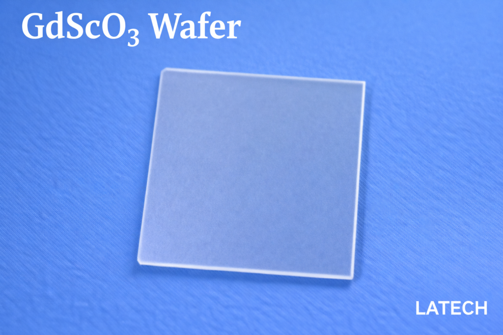
GdScO₃ Wafer (Gadolinium Scandate Wafer)
Wafer
Ternary Wafer
High-quality rare-earth scandate substrate for advanced oxide epitaxy and strain engineering
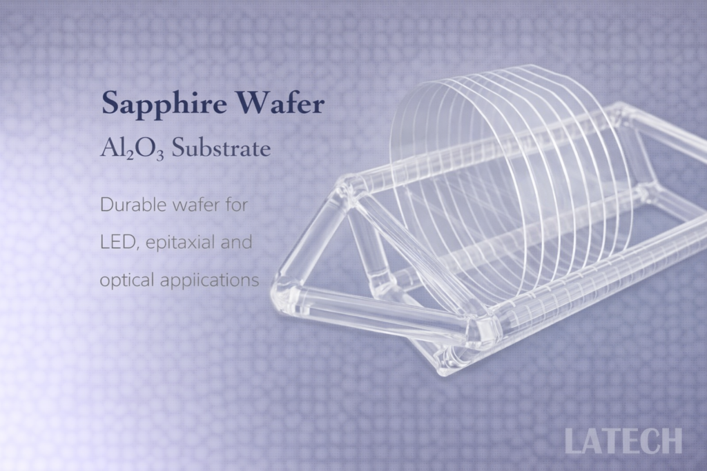
Sapphire Wafer (Al₂O₃ Substrate)
Binary Wafer
Wafer
High-quality sapphire wafers for LED, epitaxial, optical, and semiconductor applications.
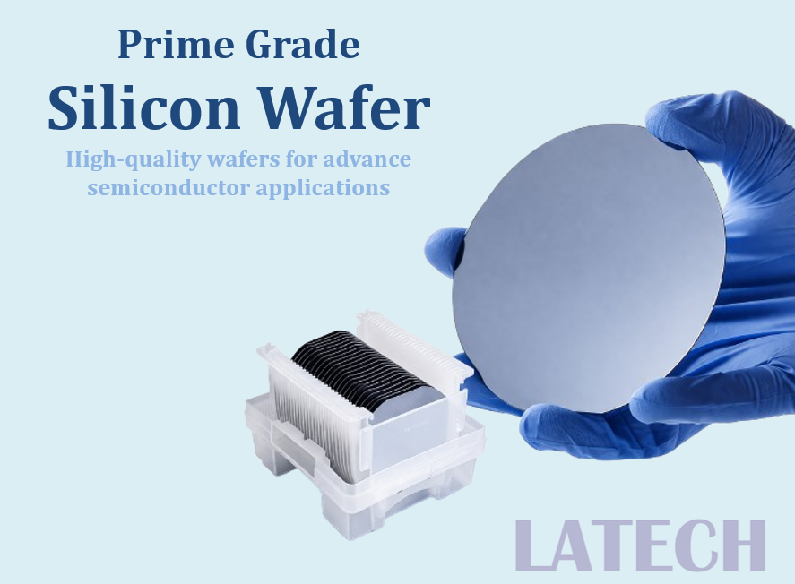
Prime Grade Silicon Wafer
Elemental Wafer
Wafer
High purity monocrystalline silicon substrate for semiconductor and research applications
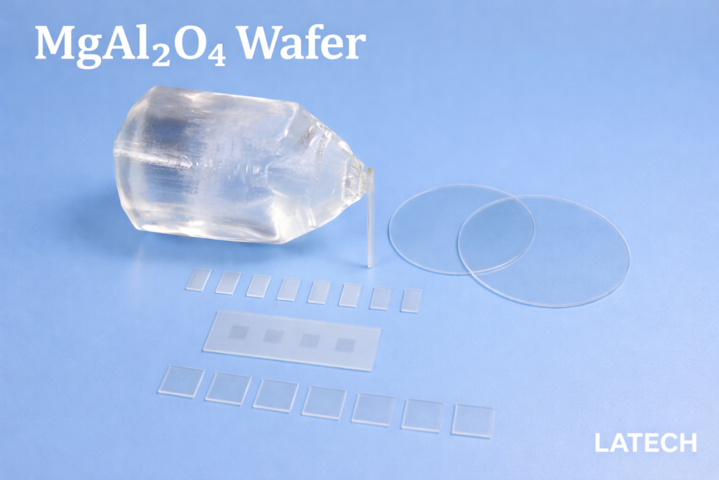
MgAl₂O₄ Wafer (Magnesium Aluminate Spinel Substrate)
Wafer
Ternary Wafer
High-performance insulating spinel substrate for microwave devices, GaN epitaxy, and advanced thin film applications

ZnO Wafer (Zinc Oxide Substrate)
Binary Wafer
Wafer
High-quality ZnO wafers for optoelectronic, piezoelectric, and thin-film applications.