Wafer
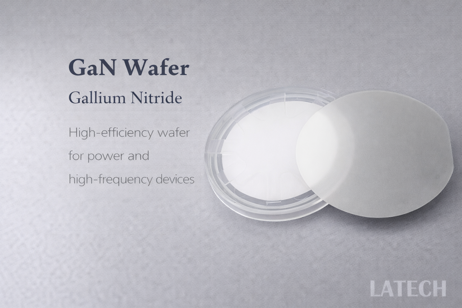
GaN Wafer (Gallium Nitride Wafer)
High-performance GaN wafers for power electronics, RF, and optoelectronic applications.
High-performance GaN wafers for power electronics, RF, and optoelectronic applications.
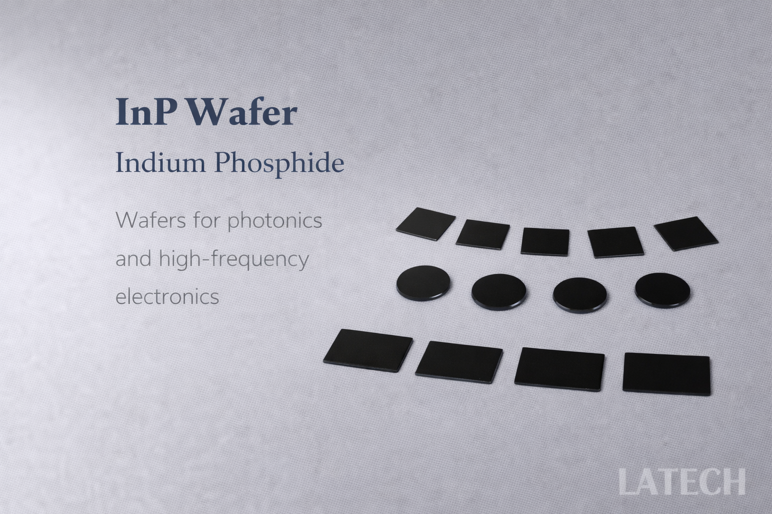
High-performance InP wafers for photonics, optoelectronics, and high-frequency applications.
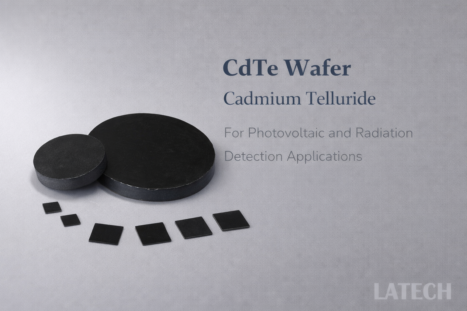
High-performance CdTe wafers for photovoltaic, infrared, and radiation detection applications.

High-quality single crystal YVO₄ substrate for optical and photonic applications
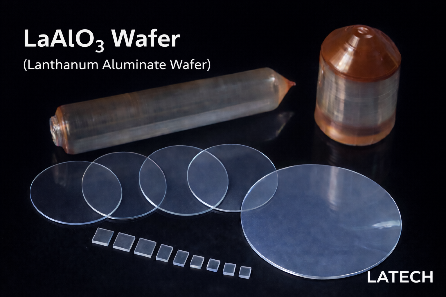
Single crystal LaAlO₃ substrate for epitaxial growth of oxide thin films and superconducting materials
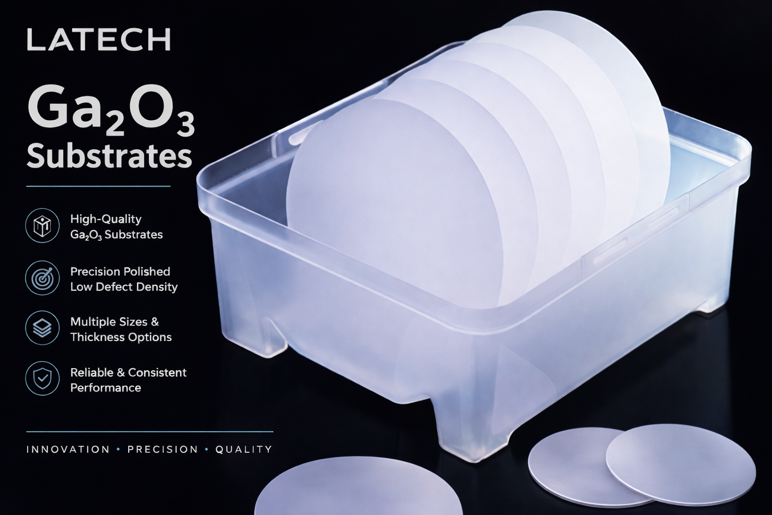
Epi-ready single crystal β-Ga₂O₃ substrate for power electronics and UV applications
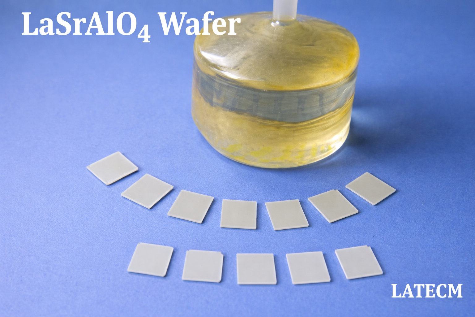
High-quality perovskite-related substrate for superconducting thin films and oxide epitaxy
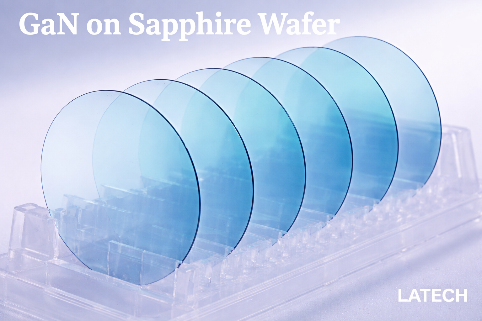
Wide bandgap semiconductor wafer for LED, RF, and high-power electronic applications
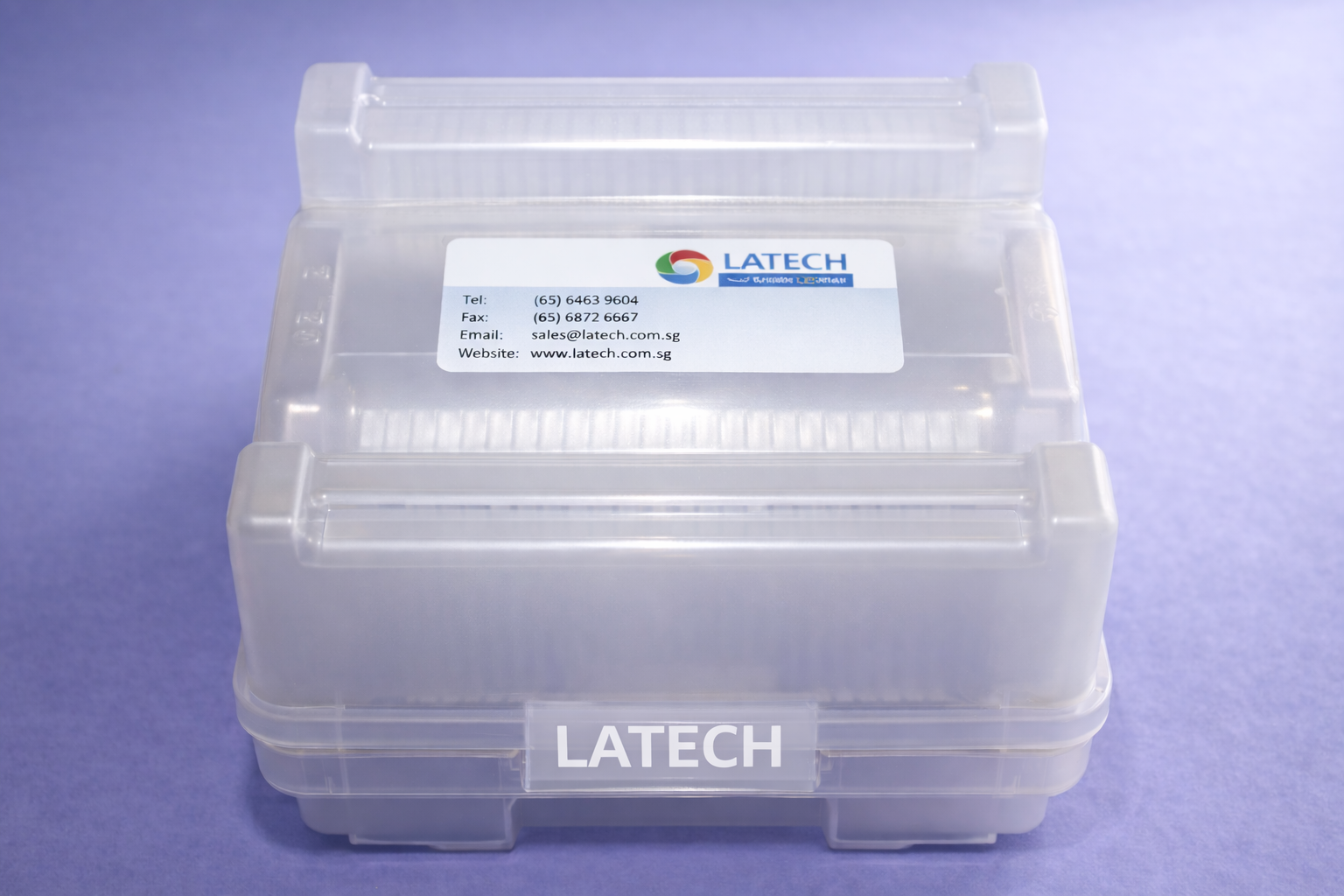
Designed for safe storage and transportation of semiconductor wafers. Suitable for general handling applications outside high-temperature or chemical processing environments.
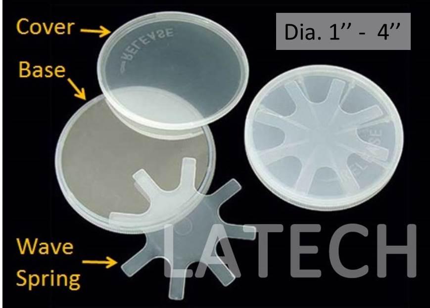
Secure storage and handling solution for semiconductor wafers from 1″ to 12″.

IC Tray Wafer Dice Antistatic Chip Box, Die Storage Tray, Die Holder Chiplet Tray
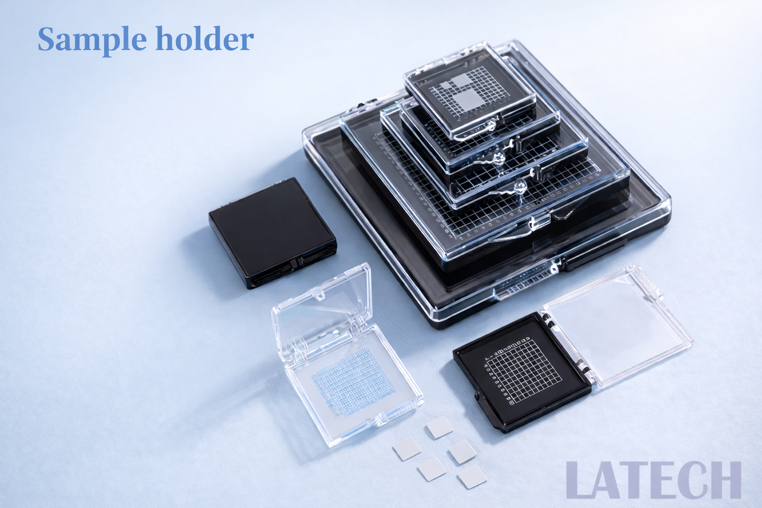
Secure storage and transportation solution for fragile chips, dies, and micro-components using adhesive gel technology.
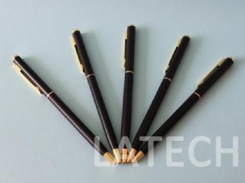
High-precision diamond scribing tool designed for wafer cutting and sample preparation.
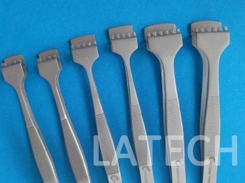
Precision tweezers for safe handling and transfer of semiconductor wafers and delicate substrates.

Silicon wafers for process evaluation, parameter testing, and R&D development
Tell us about your needs.
We will recommend the best fits for you.