
CaF₂ Wafer (Calcium Fluoride Substrate)
High-quality CaF₂ wafers for UV, IR, and high-precision optical applications.
Description
🔷 Overview
Calcium Fluoride (CaF₂) wafers are single-crystal optical substrates widely used in ultraviolet (UV), visible, and infrared (IR) optical systems.
CaF₂ offers an extremely wide transmission range (~0.13–9 μm), enabling applications from deep ultraviolet to infrared optics.
With its low refractive index (~1.43) and very low chromatic dispersion, CaF₂ is widely used in high-precision optical systems to minimize chromatic aberration and improve imaging quality.
Additionally, CaF₂ exhibits excellent optical homogeneity, high laser damage threshold, and good thermal stability, making it a preferred material for excimer lasers, lithography, and spectroscopy applications.
🔷 Key Features
- Ultra-wide transmission (UV–IR, ~0.13–9 μm)
- Low refractive index (~1.43) for optical precision
- Extremely low chromatic dispersion (high Abbe number)
- High optical homogeneity and low scattering
- High laser damage threshold (UV excimer compatible)
- Excellent transparency (>94% in UV–IR range)
- Good thermal stability and mechanical strength
🔷 Specifications
|
Product: |
Single crystal Calcium Fluoride (CaF2) wafer |
|
Purity: |
> 99.99% |
|
Material property: |
Crystal structure: cubic |
|
Lattice constant: a = 5.4626 Å |
|
|
Density: 3.18 g/cm3 |
|
|
Melting point: 1360 °C |
|
|
Solubility: 0.0017g/100g (20℃ / water) |
|
|
Transmission Band: 0.13~11.3mm |
|
|
Kirschner Hardness: 158.3 (100) |
|
|
Elastic Coefficient: C11=164, C12=53, C44=33.7 |
|
|
Visual Elasticity Limit: 36.54MPa |
|
|
Thermal Conductivity: 9.71 W/K.m |
|
|
Coefficient of Thermal expansion: 18.85 x 10⁻⁶ / ℃ |
|
|
Cleavage Plane: <111> |
|
|
Dimension: |
• 5 × 5 mm • 5 × 10 mm • 10 × 10 mm • 20 × 20 mm • Other sizes customizable |
|
Thickness: |
• 0.1 mm • 0.5 mm • 1.0 mm • 2.0 mm • Other sizes customizable |
|
Orientation: |
• <100> ± 0.5° • <110> ± 0.5° • <111> ± 0.5° • other off-angle |
|
Polishing: |
• Fine ground • Single side epi-polished • double side epi-polished |
|
Surface roughness: |
< 1 nm |
🔷 Applications
- UV optics (excimer laser systems, lithography)
- Infrared optics and spectroscopy
- Optical lenses, windows, and prisms
- Semiconductor lithography optics
- Laser systems and high-energy optics
- Aerospace and precision optical instruments
🔷 Applications
- UV optics (excimer laser systems, lithography)
- Infrared optics and spectroscopy
- Optical lenses, windows, and prisms
- Semiconductor lithography optics
- Laser systems and high-energy optics
- Aerospace and precision optical instruments
🔷 Customization Options
We support customized CaF₂ wafers based on your requirements:
- Diameter and thickness
- Orientation (<111>, <100>, <001>)
- Optical-grade polishing (SSP / DSP)
- UV-grade / IR-grade substrates
- Coated or uncoated wafers
Related Products

TiO₂ Wafer (Titanium Dioxide Substrate)
Binary Wafer
Wafer
High-quality TiO₂ substrates for optical, photonic, and thin-film applications.
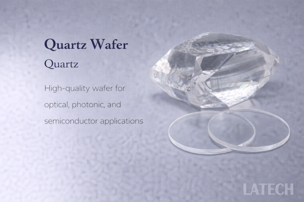
Single Crystal Quartz Wafer (SiO₂ Substrate)
Binary Wafer
Wafer
High-quality single crystal quartz wafers for optical, piezoelectric, and frequency control applications.
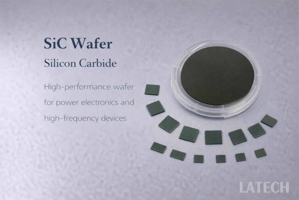
SiC Wafer (Silicon Carbide Wafer)
Binary Wafer
Wafer
High-performance SiC wafers for power electronics, high-temperature, and high-frequency applications.
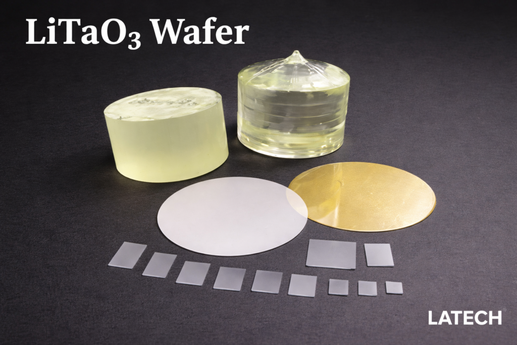
LiTaO₃ Wafer (Lithium Tantalate Substrate)
Wafer
Ternary Wafer
High-performance piezoelectric and electro-optic substrate for SAW devices, sensors, and photonic applications
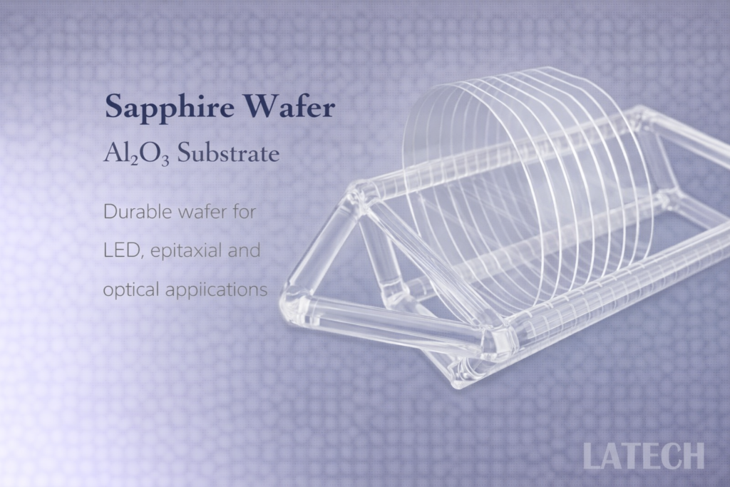
Sapphire Wafer (Al₂O₃ Substrate)
Binary Wafer
Wafer
High-quality sapphire wafers for LED, epitaxial, optical, and semiconductor applications.