
 Wafer 2")
 Wafer")

 Wafer 2")
 Wafer")
Sapphire Wafer (Al₂O₃ Substrate)
High-quality sapphire wafers for LED, epitaxial, optical, and semiconductor applications.
Description
🔷 Overview
Sapphire wafers are single-crystal aluminum oxide (Al₂O₃) substrates widely used in optoelectronics, semiconductor fabrication, and advanced optical systems.
Sapphire offers exceptional hardness (Mohs 9), high thermal stability (~2040°C melting point), and excellent optical transparency from UV to IR, making it one of the most durable and versatile substrate materials.
Due to its excellent electrical insulation and stable dielectric properties, sapphire is widely used as a substrate for high-frequency and high-power electronic devices.
Most importantly, sapphire is the primary substrate for GaN epitaxy, enabling the production of LEDs, laser diodes, and power devices.
🔷 Key Features
- Ultra-high hardness (Mohs 9, second only to diamond)
- Wide optical transmission (UV–IR: ~150 nm – 5.5 μm)
- High thermal stability (~2040°C melting point)
- Excellent electrical insulation (high resistivity)
- High thermal conductivity for heat dissipation
- Low dielectric loss for RF applications
- Strong chemical and corrosion resistance
- Available in multiple orientations (C, A, R, M planes)
🔷 Specifications
| Product: | Single crystal sapphire Al2O3 wafer |
| Purity: | >99.99% |
| Material property: | Crystal structure: hexagonal |
| Lattice constant: a = 4.76 Å, c = 12.99 Å | |
| Density: 3.97 g/cm3 | |
| Hardness: 9 mohs | |
| Thermal expansion coefficient: 7.5 × 10⁻⁶ /°C | |
| Thermal conductivity: 12.56 W/(m.K) @ 400 °C | |
| Dielectric constant: 11.58 | |
| Melting point: 2040 °C | |
| Dimension: |
• 5 × 5 × 0.5 mm • 10 × 10 × 0.5 mm • 2” × 0.43 mm • 4” × 0.65 mm • 6” × 1.0 mm • others |
| Orientation: |
• C-plane <0001> • A-plane <11-20> • R-plane <1-102> • M-plane <10-10> • Others |
| Polishing: | Single side / double side epi-polished |
| Surface roughness: | < 0.3 nm (ultra-flat for the polished surface) |
| Applications: |
• Due to the small lattice mismatch, sapphire substrates is the popular epitaxial substrate for a wide range of materials, such as group III-V gallium nitride (GaN), zinc oxide (ZnO), superconductor, magnetic, etc • Sapphire is the epi-substrate for commercial light emitting diode (LED) industry • Sapphire is chemically and physically stable |
| Useful Links: | • Properties and applications of sapphire (Al2O3) |

🔷 Applications
- GaN-based LEDs and laser diodes
- Power electronics and RF devices
- Optical windows (UV / IR / laser systems)
- Semiconductor epitaxy substrates
- Silicon-on-sapphire (SOS) circuits
- Sensors and high-temperature devices
- Aerospace and harsh-environment optics
🔷 Why Choose Sapphire
- Ideal substrate for GaN epitaxy and LED production
- Extremely durable and scratch-resistant (Mohs 9)
- Wide optical transparency from UV to IR
- High thermal conductivity for efficient heat dissipation
- Excellent electrical insulation for high-frequency electronics
🔷 Customization Options
We support customized sapphire wafers based on your requirements:
- Orientation (C, A, R, M plane)
- Diameter and thickness
- Surface finish (SSP / DSP / epi-ready)
- Ultra-thin wafers
- Optical-grade or semiconductor-grade
Related Products
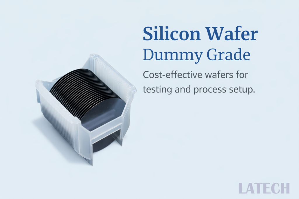
Dummy Grade Silicon Wafer
Elemental Wafer
Wafer
Cost-effective silicon wafer for process testing, equipment calibration, and non-critical applications
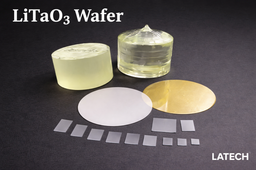
LiTaO₃ Wafer (Lithium Tantalate Substrate)
Wafer
Ternary Wafer
High-performance piezoelectric and electro-optic substrate for SAW devices, sensors, and photonic applications

DyScO₃ Wafer (Dysprosium Scandate Wafer)
Wafer
Ternary Wafer
High-quality rare-earth scandate substrate for oxide epitaxy and strain engineering

SrTiO₃ Wafer (Strontium Titanate Wafer)
Wafer
Ternary Wafer
High-quality insulating perovskite oxide substrate for epitaxial growth and advanced oxide thin film applications

LiAlO₂ Wafer (Lithium Aluminate Substrate)
Wafer
Ternary Wafer
High-performance substrate for GaN epitaxy, superconducting films, and microwave applications