
 2")
 3")
 4")


 2")
 3")
 4")

Prime Grade Silicon Wafer
High purity monocrystalline silicon substrate for semiconductor and research applications
Description
🔷 Product Overview
A silicon wafer is a thin slice of high-purity single-crystal silicon used as the substrate for semiconductor device fabrication, including integrated circuits (ICs), MEMS devices, sensors, and photovoltaic cells.
Prime grade wafers offer superior surface quality, low defect density, and tight control of electrical properties, making them suitable for advanced fabrication and high-performance applications.
🔷 Key Specifications
| Product: | Monocrystalline Silicon (Si) wafer |
| Grade: | IC prime grade |
| Purity: | >99.999999999% (11N) |
| Growth Method: | • CZ wafers are suitable for general semiconductor applications • FZ wafers are recommended for high resistivity, RF and power devices |
| Diamension |
Standard dimensions: • 1” × 0.5 mm • 2” × 0.28 / 0.4 / 0.5 mm • 3” × 0.38 mm • 4” × 0.525 mm • 5” × 0.6 mm • 6” × 0.625 mm • 8” × 0.725 mm Other diameters and thicknesses available • We provide small-scale non-standard wafers for research / testing purposes. |
| Orientation: | <100> / <110> / <111> / off-axis / others |
| Conductive type: |
• Undoped (also called intrinsic, native) type • N-type: phosphor (P) /Arsenic doped • P-type: boron (B) doped |
| Resistivity: |
Standard resistivity for undoped wafers: • 3000 – 6000 Ω·cm Standard resistivity for n-/ p-type wafers: • 0.001 – 0.009 Ω·cm • 1 – 10 Ω·cm • 10 – 20 Ω·cm • 90 – 100 Ω·cm Other resistivity available |
| Polishing: |
• As-cut wafers without polishing • Single side epi-polished • Double side epi-polished |
| Surface roughness: | < 0.5 nm |
| Flat / Notch | SEMI standard |
| Remarks: | Si wafer with functional layers available (thermal oxide SiO2, silicon nitride Si3N4, etc) |
🔷 Growth Method
Silicon wafers are produced using different crystal growth methods, which directly affect purity and electrical properties:
- Czochralski (CZ):
Standard industrial method, cost-effective, widely used for most semiconductor applications - Float Zone (FZ):
Ultra-high purity, low oxygen content, ideal for high resistivity and advanced research applications
👉 FZ wafers are recommended for high-frequency, power electronics, and precision research applications.
🔷 Manufacturing Process
Typical silicon wafer production includes:
- Crystal growth (CZ / FZ)
- Ingot shaping and slicing
- Edge grinding
- Lapping and chemical etching
- Chemical Mechanical Polishing (CMP)
This process ensures excellent flatness, uniform thickness, and defect-free surfaces.
🔷 Applications
- Semiconductor device fabrication (IC)
- MEMS and microfabrication
- Photovoltaic research
- Sensors and optoelectronics
- University and R&D laboratories
🔷 Customization Available
We provide customized silicon wafers based on your requirements:
- Diameter & thickness
- Orientation & off-cut angle
- Resistivity & dopant type
- Single-side / double-side polishing
- Oxide / epitaxial / special coatings
👉 Please contact us for tailored specifications.
Related Products
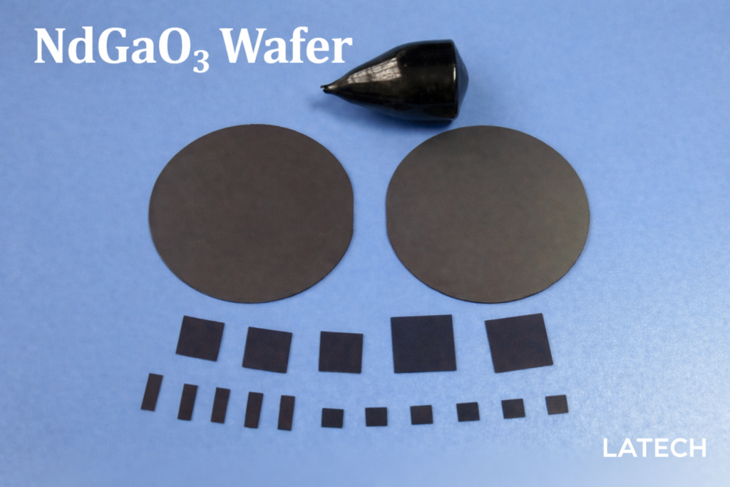
NdGaO₃ Wafer (Neodymium Gallate Substrate)
Wafer
Ternary Wafer
High-quality perovskite oxide substrate for superconducting, magnetic, and epitaxial thin film applications
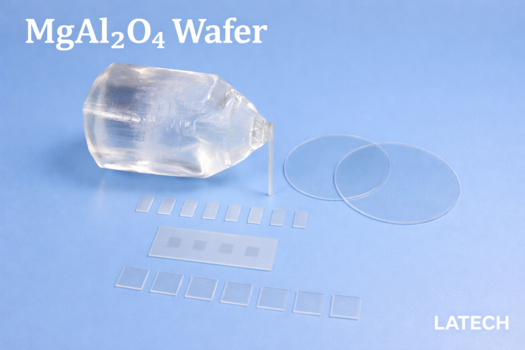
MgAl₂O₄ Wafer (Magnesium Aluminate Spinel Substrate)
Wafer
Ternary Wafer
High-performance insulating spinel substrate for microwave devices, GaN epitaxy, and advanced thin film applications
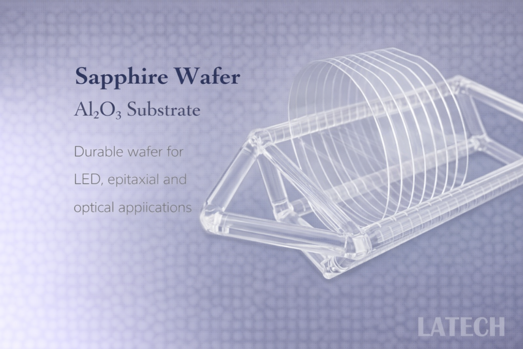
Sapphire Wafer (Al₂O₃ Substrate)
Binary Wafer
Wafer
High-quality sapphire wafers for LED, epitaxial, optical, and semiconductor applications.
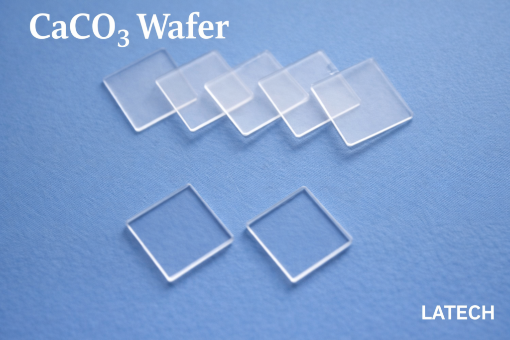
CaCO₃ Wafer (Calcium Carbonate Wafer)
Wafer
Ternary Wafer
High birefringence optical crystal substrate for polarization and photonic applications

TiO₂ Wafer (Titanium Dioxide Substrate)
Binary Wafer
Wafer
High-quality TiO₂ substrates for optical, photonic, and thin-film applications.