
GaN on Sapphire Wafer
Wide bandgap semiconductor wafer for LED, RF, and high-power electronic applications
Description
🔷 Overview
GaN on Sapphire wafer is a widely used epitaxial structure consisting of a gallium nitride (GaN) layer grown on a sapphire (Al₂O₃) substrate.
GaN is a wide bandgap semiconductor (~3.4 eV) with high breakdown voltage and excellent thermal stability, while sapphire provides a cost-effective and reliable substrate for large-scale production.
This combination makes GaN on sapphire an industry-standard platform for LEDs, RF devices, and power electronics.
🔷 Key Features
• Wide bandgap (~3.4 eV) for high-power applications
• High breakdown voltage and high-temperature stability
• Mature and cost-effective sapphire substrate
• Suitable for high-frequency and high-power devices
• Available in doped and undoped configurations
• Epi-ready surface with low defect density
🔷 Specifications
|
Product |
Gallium Nitride on Sapphire wafer / GaN on Sapphire wafer |
|
Dopant and Conductivity |
• N-type/Si-doped • N-type/Un-doped • P-type/Mg-doped |
|
Orientation |
C-plane, <0001> |
|
Standard Size |
• Dia 2” (50.8 mm) • Dia 4” (100 mm) |
|
Thickness: |
• 430 um • 650 um |
|
GaN thin film |
• 4.5 um • 20 um |
|
Resistivity/Carrier concentration |
• < 0.05 ohm-cm / > 1 10E18 /cm3 • < 0.5 ohm-cm / < 5x10E17 /cm3 • < 10 ohm-cm / > 6x10E16 /cm3 |
|
Dislocation density |
<5x10E8 cm-2 |
|
Usable area |
>90% |
|
Polishing: |
• Single side epi-polished • double side epi-polished |
|
Surface roughness |
< 0.5 nm |
🔷 Applications
• LED (blue / green / UV LEDs)
• RF and microwave devices
• High Electron Mobility Transistors (HEMT)
• Power electronics (high voltage / high frequency)
• Photonics and optoelectronics
🔷 Why Choose GaN on Sapphire
• Industry-standard platform for LED manufacturing
• Lower cost compared to SiC and bulk GaN
• Mature and scalable epitaxial technology
• Suitable for both research and mass production
🔷 Customization Options
• GaN thickness customization
• Doping type and concentration
• Orientation and off-cut
• Epi-structure design (AlN buffer / AlGaN layers)
• Device-ready wafers (HEMT / LED structures)
Related Products
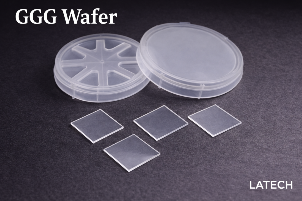
GGG Wafer (Gadolinium Gallium Garnet, Gd₃Ga₅O₁₂ Wafer)
Ternary Wafer
Wafer
High-quality garnet substrate for magnetic thin films and oxide epitaxy
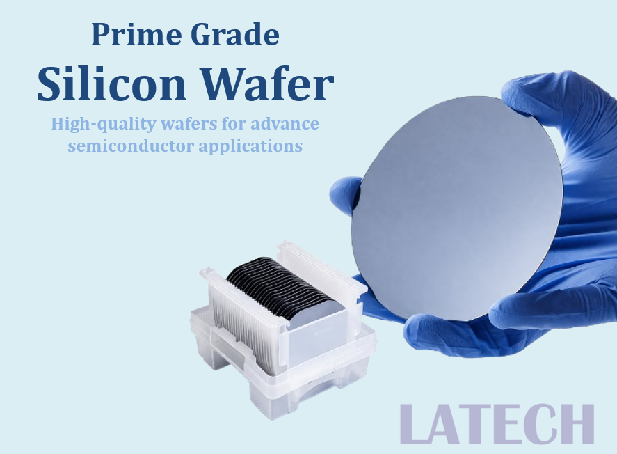
Prime Grade Silicon Wafer
Elemental Wafer
Wafer
High purity monocrystalline silicon substrate for semiconductor and research applications
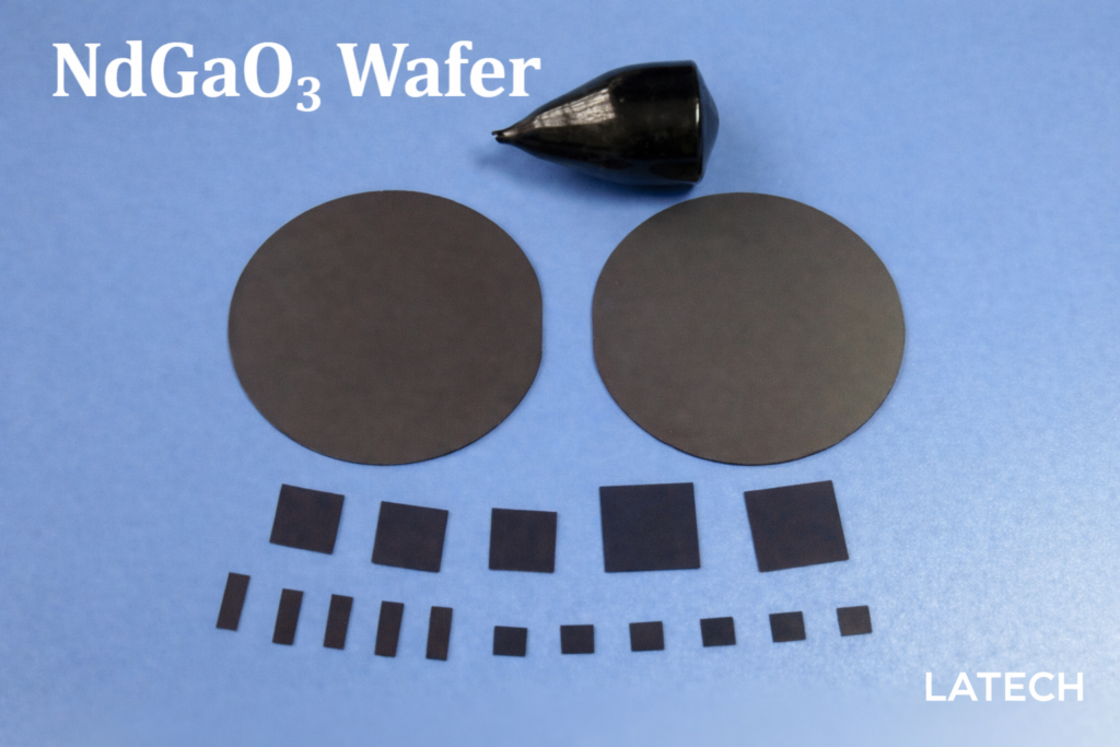
NdGaO₃ Wafer (Neodymium Gallate Substrate)
Wafer
Ternary Wafer
High-quality perovskite oxide substrate for superconducting, magnetic, and epitaxial thin film applications

ZnO Wafer (Zinc Oxide Substrate)
Binary Wafer
Wafer
High-quality ZnO wafers for optoelectronic, piezoelectric, and thin-film applications.

DyScO₃ Wafer (Dysprosium Scandate Wafer)
Wafer
Ternary Wafer
High-quality rare-earth scandate substrate for oxide epitaxy and strain engineering