
InP Wafer (Indium Phosphide Wafer)
High-performance InP wafers for photonics, optoelectronics, and high-frequency applications.
Description
🔷 Overview
Indium Phosphide (InP) wafers are III–V compound semiconductor substrates widely used in photonics, optoelectronics, and high-speed electronic devices.
InP features a direct bandgap (~1.34–1.35 eV), enabling efficient light emission and detection, making it an ideal material for lasers, photodetectors, and optical communication systems.
Compared with silicon, InP offers significantly higher electron mobility, allowing superior performance in high-frequency and high-speed devices such as RF amplifiers and millimeter-wave systems.
In addition, InP substrates combine strong optical properties with high-speed electronic performance, making them a key material for photonic integrated circuits (PICs) and next-generation communication technologies.
🔷 Key Features
- Direct bandgap (~1.34–1.35 eV) for efficient light emission
- High electron mobility for high-speed electronics
- Excellent performance in photonics and optical communication
- Low noise characteristics for RF and microwave devices
- Suitable for photonic integrated circuits (PICs)
- Good radiation resistance for aerospace applications
- Stable operation at high frequencies and elevated temperatures
🔷 Specifications
|
Product: |
Single crystal InP wafer |
|
Material property: |
Crystal structure: Cubic |
|
Lattice constant: a = 5.4505 Å |
|
|
Density: 4.81 g/cm3 |
|
|
Melting Point: 1062 °C |
|
|
Dislocation density: < 5000 cm^-2 |
|
|
Hardness: 3 Mohs |
|
|
Growth Method: LEC |
|
|
Conductive type/dopant / carrier concentration cm-3 / Mobility (cm2/V.s) |
• Semi-Insulating / Te / 107-108 / ≥ 1000 • N-type / Undoped / (0.4-3) × 1016 / (3.5-4) × 103 • N-type / S / (0.8-6) × 1018 / (1.5-3.5) × 103 • P-type / Zn / (0.6-6) × 1018 / 50-70 |
|
Dimension: |
• 5 × 5 × 0.5 mm • 5 × 10 × 0.5 mm • 10 × 10 × 0.5 mm • 20 × 20 × 0.5 mm • Other sizes customizable |
|
Orientation: |
• <100> ± 0.5° • <111> ± 0.5° |
|
Polishing: |
• Fine ground • Single side epi-polished • double side epi-polished |
|
Surface roughness: |
< 0.5 nm |
🔷 Applications
- Fiber-optic communication systems
- Laser diodes and optical transmitters
- Photodetectors and optical sensors
- High-frequency and RF electronics
- Photonic integrated circuits (PICs)
- Satellite and aerospace systems
- Semiconductor and research applications
🔷 Why Choose InP Over Silicon
- Direct bandgap enables efficient light emission (unlike silicon)
- Higher electron mobility for faster device performance
- Better suited for photonics and optical communication systems
- Lower signal loss in high-frequency applications
🔷 Customization Options
- Size and thickness
- Orientation and off-angle
- Doping type and resistivity
- Surface polishing (SSP / DSP)
- Research-grade or device-grade wafers
Related Products
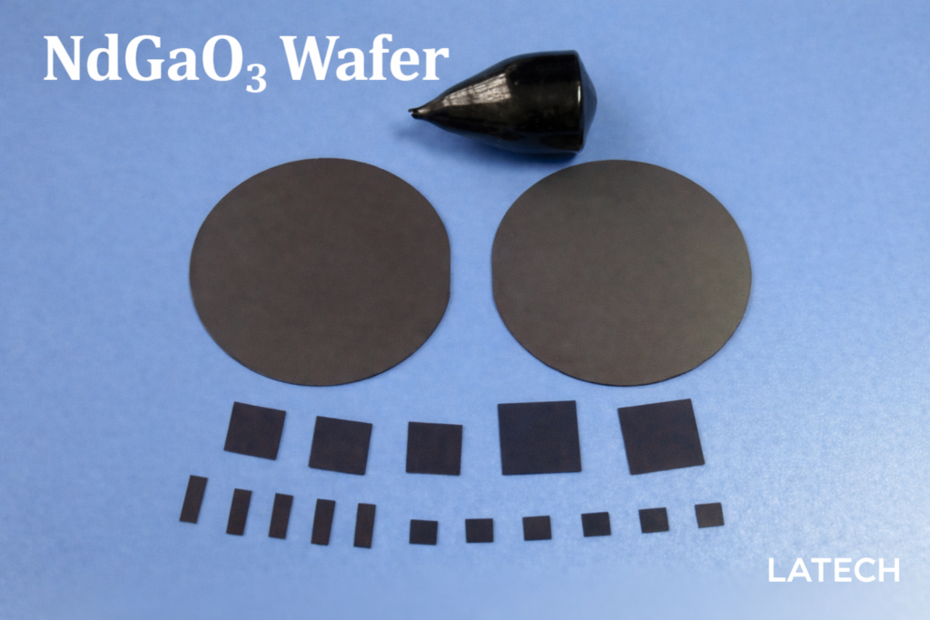
NdGaO₃ Wafer (Neodymium Gallate Substrate)
Ternary Wafer
Wafer
High-quality perovskite oxide substrate for superconducting, magnetic, and epitaxial thin film applications
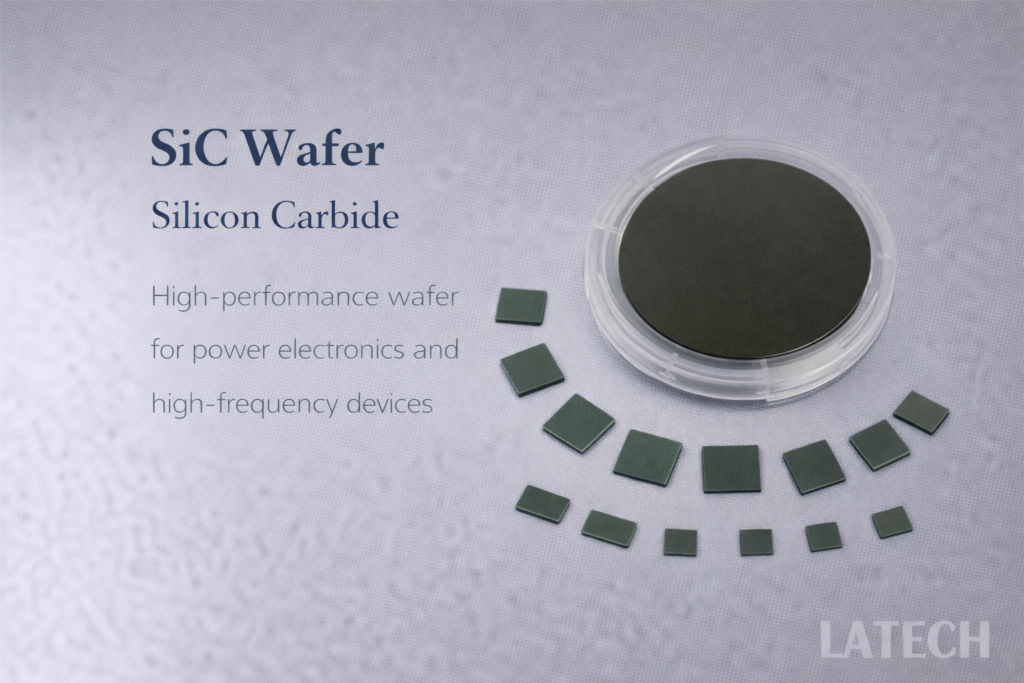
SiC Wafer (Silicon Carbide Wafer)
Binary Wafer
Wafer
High-performance SiC wafers for power electronics, high-temperature, and high-frequency applications.
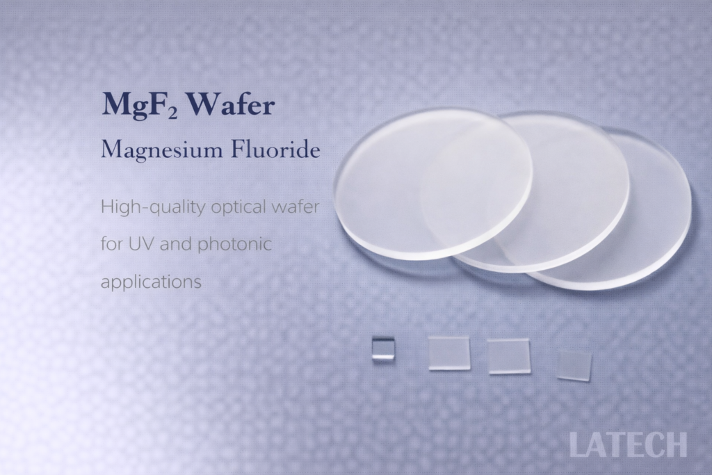
MgF₂ Wafer (Magnesium Fluoride Substrate)
Binary Wafer
Wafer
High-quality MgF₂ wafers for UV, optical, and photonic applications.
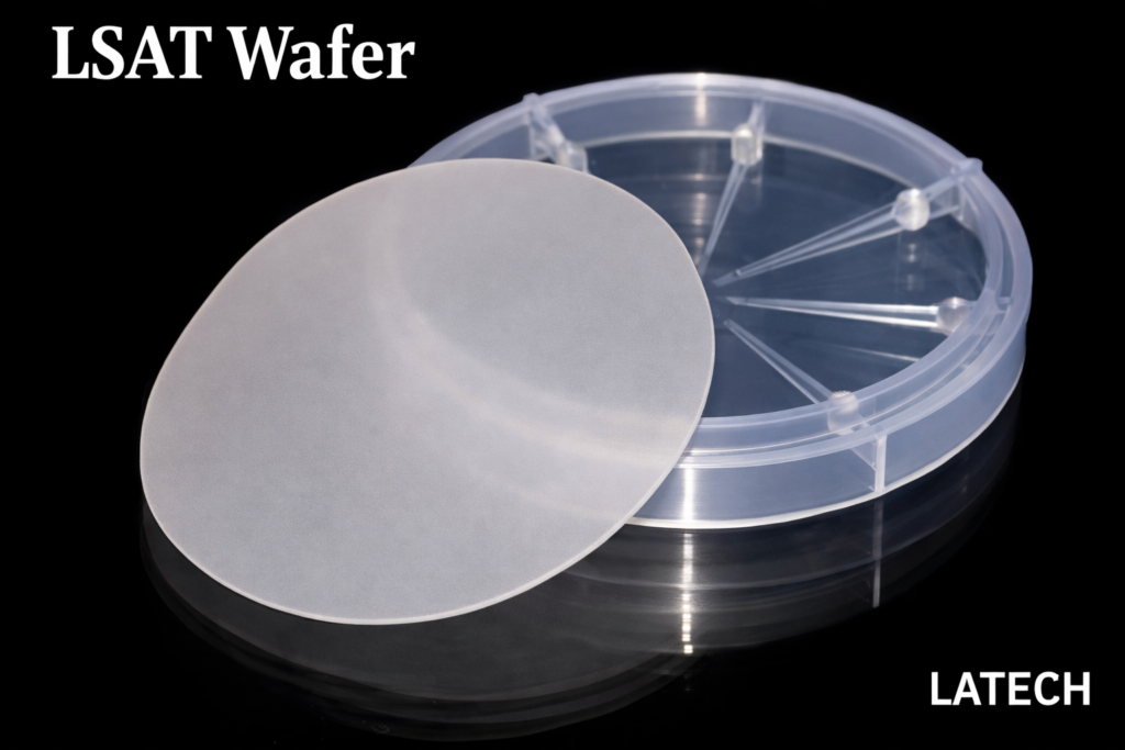
LSAT Wafer
Wafer
Other Wafers
Lattice-matched perovskite substrate for oxide epitaxy and superconducting thin films
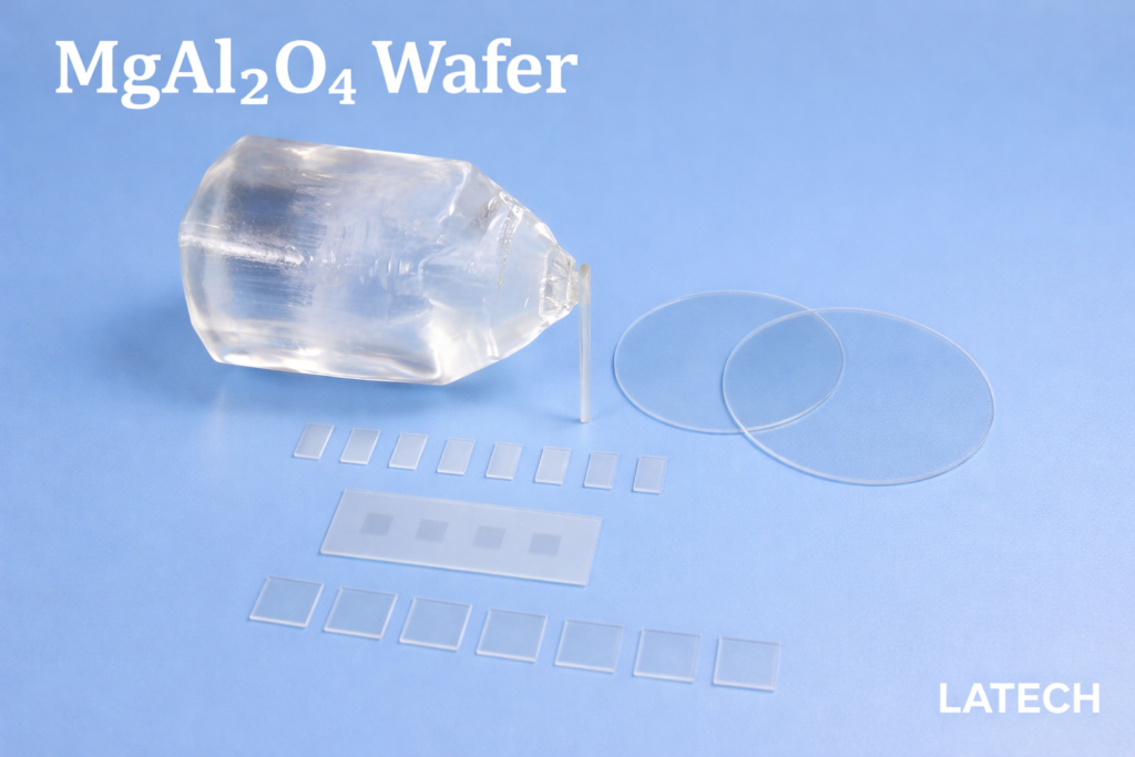
MgAl₂O₄ Wafer (Magnesium Aluminate Spinel Substrate)
Wafer
Ternary Wafer
High-performance insulating spinel substrate for microwave devices, GaN epitaxy, and advanced thin film applications