
Germanium Wafer (Ge Wafer)
High-purity germanium wafers for infrared, optical, and semiconductor applications.
Description
🔷 Overview
Germanium wafers are widely used in infrared optics, semiconductor research, and advanced electronic applications.
Our single-crystal germanium (Ge) wafers offer high purity, excellent surface quality, and reliable performance for both R&D and industrial processes.
Epi-ready polished surfaces and customizable specifications make them suitable for a wide range of applications including detectors, optoelectronics, and thin-film deposition.
🔷 Key Features
- High-purity single-crystal germanium wafer (up to 6N)
- Excellent surface quality with epi-ready polishing
- Available in multiple orientations and doping types
- Low defect density with controlled EPD
- Customizable dimensions, thickness, and specifications
- Suitable for both research and industrial applications
🔷 Specifications
| Product: | Germanium (Ge) wafer |
| Purity: | 99.9999% (6N) |
| Material property: | Crystal structure: cubic |
| Lattice constant: a = 5.6576 Å | |
| Bandgap: 0.67 eV (300 K) | |
| Melting point: 937.4 °C | |
| Dimension: |
• 2” × 0.4 mm, 2” × 0.5 mm • 4” × 0.5 mm • Other dimensions available |
| Orientation: | <100> / <110> / <111> / others |
| Conductive type: | Undoped native / n-type / p-type |
| Resistivity: |
• 1 – 50 Ω·cm for undoped native wafer (exhibiting n-type behavior) • 0.01 – 0.07 Ω·cm for n-type and p-type doped wafers |
| Etch pit density (EPD): |
• Low 1000 – 5000 cm-2 • High < 10000 cm-2 |
| Polishing: | Single side / double side epi-polished |
| Surface roughness: | < 0.5 nm |
🔷 Applications
- Infrared optics and imaging systems
- Semiconductor substrates
- Photodetectors and sensors
- Solar cell research
- Thin film deposition and epitaxy
- Optoelectronic devices
🔷 Customization Options
We support customized germanium wafers based on your specific requirements:
- Diameter and thickness
- Orientation and off-cut angle
- Doping type and resistivity
- Surface finish (SSP / DSP)
- Special polishing or epi-ready surface
Related Products
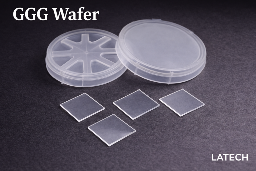
GGG Wafer (Gadolinium Gallium Garnet, Gd₃Ga₅O₁₂ Wafer)
Ternary Wafer
Wafer
High-quality garnet substrate for magnetic thin films and oxide epitaxy
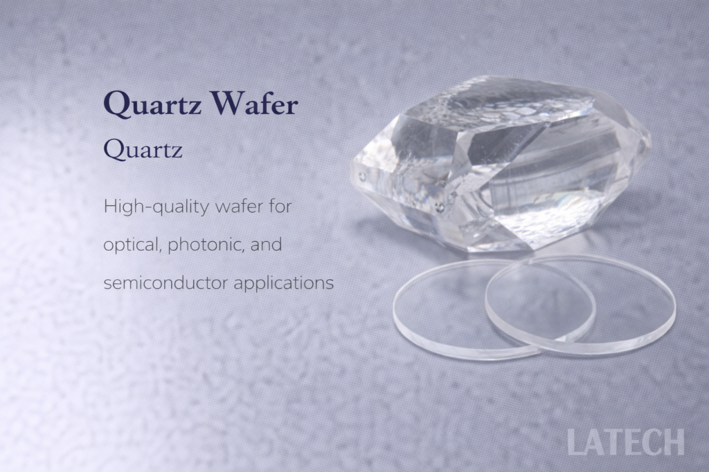
Single Crystal Quartz Wafer (SiO₂ Substrate)
Binary Wafer
Wafer
High-quality single crystal quartz wafers for optical, piezoelectric, and frequency control applications.
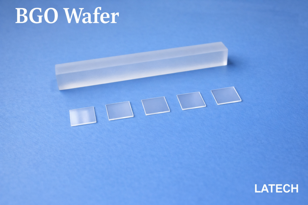
BGO Wafer (Bismuth Germanate, Bi₄Ge₃O₁₂ Wafer)
Wafer
Ternary Wafer
High-density scintillation crystal substrate for radiation detection and optoelectronic applications
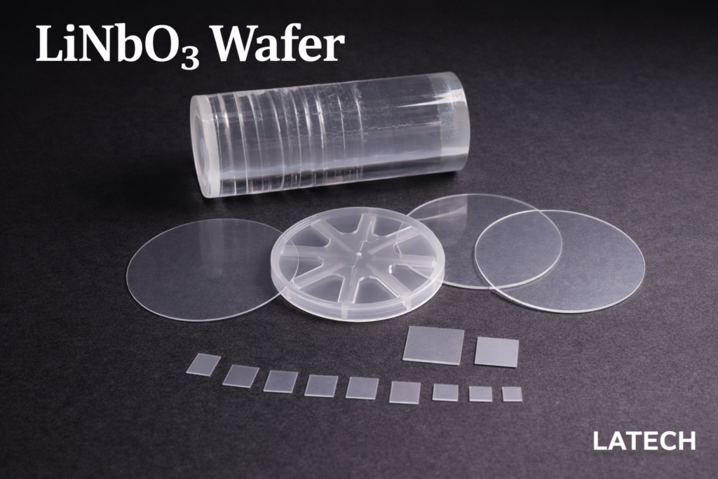
LiNbO₃ Wafer (Lithium Niobate Substrate)
Wafer
Ternary Wafer
High-performance electro-optic and piezoelectric substrate for photonics, modulators, and SAW devices

TiO₂ Wafer (Titanium Dioxide Substrate)
Binary Wafer
Wafer
High-quality TiO₂ substrates for optical, photonic, and thin-film applications.