
CdTe Wafer (Cadmium Telluride Wafer)
High-performance CdTe wafers for photovoltaic, infrared, and radiation detection applications.
Description
🔷 Overview
Cadmium Telluride (CdTe) wafers are II–VI compound semiconductor substrates widely used in photovoltaic, optoelectronic, and radiation detection applications.
CdTe features a near-ideal direct bandgap (~1.5 eV) that closely matches the solar spectrum, enabling highly efficient energy conversion. It also exhibits a very high absorption coefficient (>10⁴–10⁵ cm⁻¹), allowing efficient light absorption even with thin material layers.
In addition, its high atomic number and high resistivity make CdTe an excellent material for X-ray and gamma-ray detection, capable of operating at room temperature without complex cooling systems.
🔷 Key Features
- Direct bandgap (~1.5 eV) ideal for photovoltaic applications
- High absorption coefficient (>10⁴–10⁵ cm⁻¹)
- Efficient light absorption with thin material layers
- Requires significantly thinner absorber layers compared to silicon
- High atomic number for radiation detection
- Capable of room-temperature operation
- High resistivity and excellent stability
- Suitable for optoelectronic and detector applications
🔷 Specifications
|
Product: |
Single crystal Cadmium Telluride (CdTe) wafer |
|
Material property: |
Crystal structure: Cubic |
|
Lattice constant: a = 6.483 Å |
|
|
Density: 5.851 g/cm3 |
|
|
Melting Point: 1047 °C |
|
|
Thermal Conductivity: 6.3 W/K.m at 300 K |
|
|
Thermal Expansion Coefficient: 5.9 × 10⁻⁶ /K |
|
|
Transmission Range: ~0.85 µm – 25 µm (IR transparent) |
|
|
Refractive Index (n): ~2.7 at 10 µm |
|
|
Growth Method: PVT |
|
|
Conductive type
|
• Un-doped • P-type |
|
Dimension: |
• 5 × 5 × 0.5 mm • 5 × 10 × 0.5 mm • 10 × 10 × 0.5 mm • 20 × 20 × 0.5 mm • Other sizes customizable |
|
Orientation: |
• <100> ± 0.5° • <001> ± 0.5° • <110> ± 0.5° • <111> ± 0.5° |
|
Polishing: |
• Fine ground • Single side epi-polished • double side epi-polished |
|
Surface roughness: |
< 0.5 nm |
🔷 Applications
- Thin-film solar cells (photovoltaics)
- Infrared and optical devices
- X-ray and gamma-ray detectors
- Medical imaging systems
- Semiconductor and optoelectronic research
🔷 Customization Options
We support customized CdTe wafers based on your requirements:
- Diameter and thickness
- Orientation and off-angle
- Doping type and resistivity
- Surface polishing (SSP / DSP)
- Detector-grade or photovoltaic-grade material
Related Products
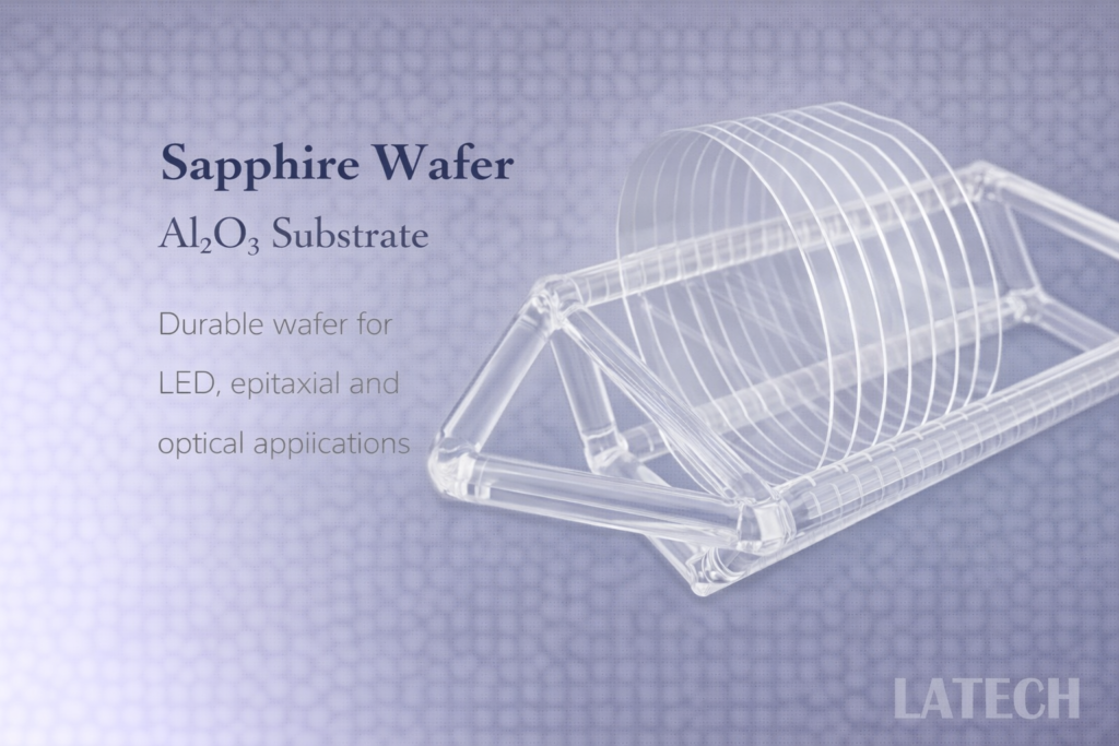
Sapphire Wafer (Al₂O₃ Substrate)
Binary Wafer
Wafer
High-quality sapphire wafers for LED, epitaxial, optical, and semiconductor applications.
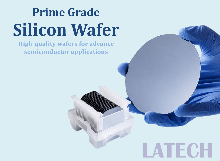
Prime Grade Silicon Wafer
Elemental Wafer
Wafer
High purity monocrystalline silicon substrate for semiconductor and research applications
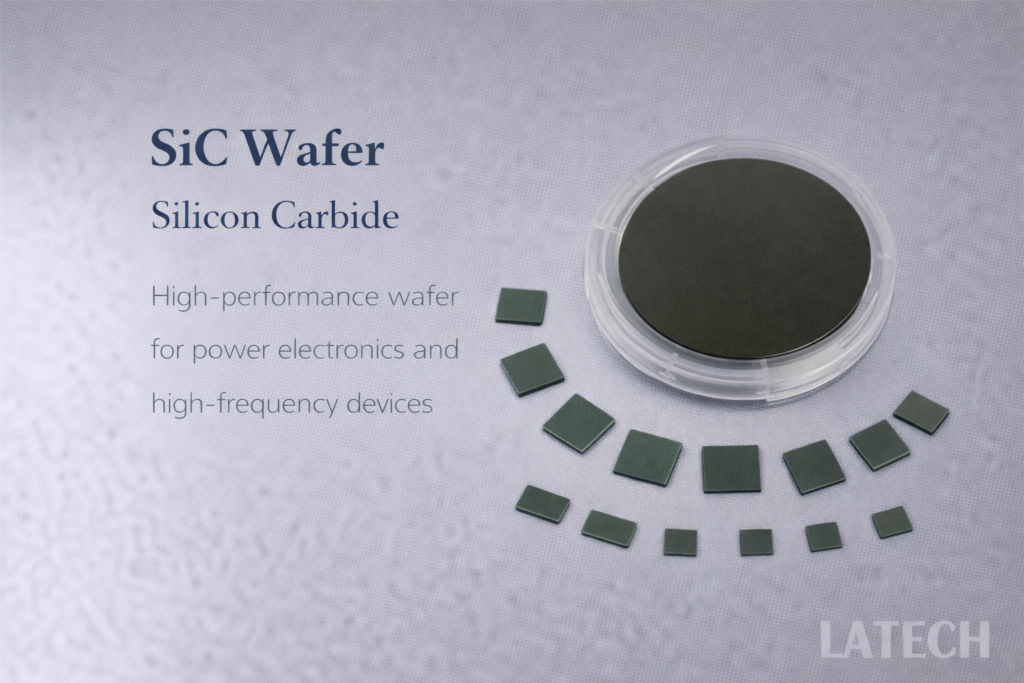
SiC Wafer (Silicon Carbide Wafer)
Binary Wafer
Wafer
High-performance SiC wafers for power electronics, high-temperature, and high-frequency applications.

SiO₂ Coated Silicon Wafers (Thermal Oxide Wafers)
Elemental Wafer
Wafer
High-quality silicon wafers with precisely controlled oxide layers for semiconductor and microfabrication applications.
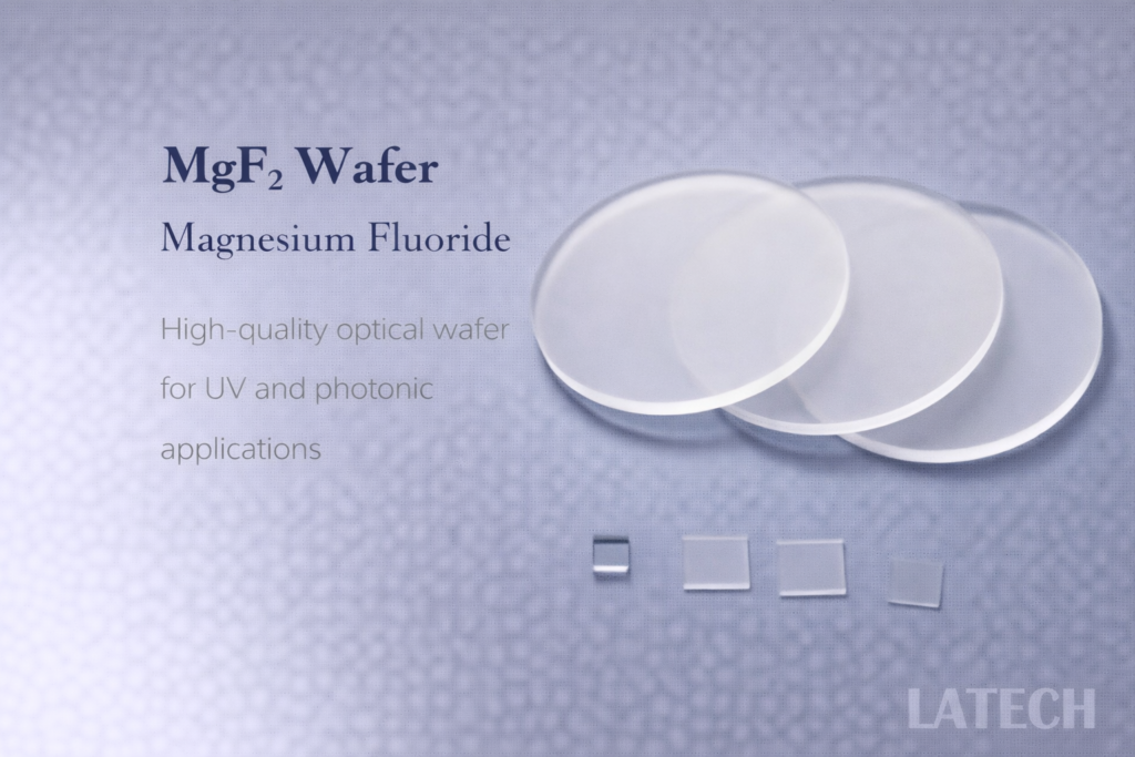
MgF₂ Wafer (Magnesium Fluoride Substrate)
Binary Wafer
Wafer
High-quality MgF₂ wafers for UV, optical, and photonic applications.