
Single Crystal Quartz Wafer (SiO₂ Substrate)
High-quality single crystal quartz wafers for optical, piezoelectric, and frequency control applications.
Description
🔷 Overview
Single crystal quartz wafers are high-purity silicon dioxide (SiO₂) substrates precisely cut and polished from synthetic quartz crystals.
Quartz exhibits excellent piezoelectric properties, optical transparency, and high thermal stability, making it one of the most important materials for frequency control and precision electronic applications.
In addition, quartz wafers provide high chemical resistance and low thermal expansion, ensuring stable performance in optical, semiconductor, and harsh-environment applications.
Due to their uniform crystal structure and customizable cut orientations, quartz wafers are widely used in oscillators, sensors, optical devices, and thin-film processing.
🔷 Key Features
- Excellent piezoelectric properties for frequency control devices
- High optical transparency from UV to IR range
- Low thermal expansion for stable performance
- High chemical and environmental resistance
- High Q factor for resonator applications
- Electrical insulation with low conductivity
- Available in multiple crystallographic cuts (AT, ST, Z, X, Y)
🔷 Specifications
|
Material |
Synthetic Quartz Crystal |
|||
|
Cutting Angle |
X/Y/Z/AT32°/33°/35°/36°/BT/ST42.75°-cut etc per Customized |
|||
|
Diameter/size |
3” (76.2mm) |
4”(100mm) |
6″(150mm) |
8″(200mm) |
|
Tol(±) |
<0.20 mm |
|||
|
Thinnest Thickness |
0.08mm Min-up |
0.10mm Min-up |
0.20mm Min -up |
0.35mm Min- |
|
Primary Flat |
22mm |
32mm |
42.5mm |
57.5mm or notch |
|
LTV (5mmx5mm) |
<1.5µm |
|||
|
TTV |
<1.5~3 µm |
|||
|
Bow |
-30<bow<30 |
|||
|
Warp |
<40µm |
|||
|
PLTV(<0.5um) |
≥95%(5mm*5mm) |
|||
|
Orientation Flat |
All available |
|||
|
Surface Type |
Single Side Polished /Double Sides Polished |
|||
|
Polished side Ra |
<0.5nm or specific per requested |
|||
|
Back Side Criteria |
General is 0.2-0.5µm or as customized |
|||
|
Edge Criteria |
R=0.2mm or Bullnose |
|||
|
Material Property |
ECD |
Better than grade 4 |
||
|
Inclusion |
Better than grade II |
|||
|
Q-Value |
Better than grade C |
|||
|
Wafer Surface Criteria |
Particles ¢>0.3 µ m |
<= 30 |
||
|
Scratch , Chipping |
None |
|||
|
Defect |
No edge cracks, scratches, saw marks, stains |
|||
|
Packaging |
Qty/Wafer box |
25pcs per box Semi Standard |
||

🔷 Applications
- Frequency control devices (oscillators, resonators)
- Surface acoustic wave (SAW) devices
- Optical components (windows, waveplates, filters)
- Semiconductor processing and photolithography
- MEMS and sensors
- RF and wireless communication systems
🔷 Why Choose Quartz
- Unique piezoelectric effect enables precise frequency control
- High optical transparency for photonic applications
- Excellent stability across temperature and environment
- Highly reliable material for long-term electronic devices
- Suitable for both optical and electronic applications
🔷 Customization Options
We support customized quartz wafers based on your requirements:
- Crystal orientation (AT, ST, Z, X, Y cut)
- Diameter and thickness
- Surface polishing (SSP / DSP)
- Optical-grade or SAW-grade wafers
- Seeded or seedless quartz
Related Products

SrTiO₃ Wafer (Strontium Titanate Wafer)
Wafer
Ternary Wafer
High-quality insulating perovskite oxide substrate for epitaxial growth and advanced oxide thin film applications

LiAlO₂ Wafer (Lithium Aluminate Substrate)
Wafer
Ternary Wafer
High-performance substrate for GaN epitaxy, superconducting films, and microwave applications
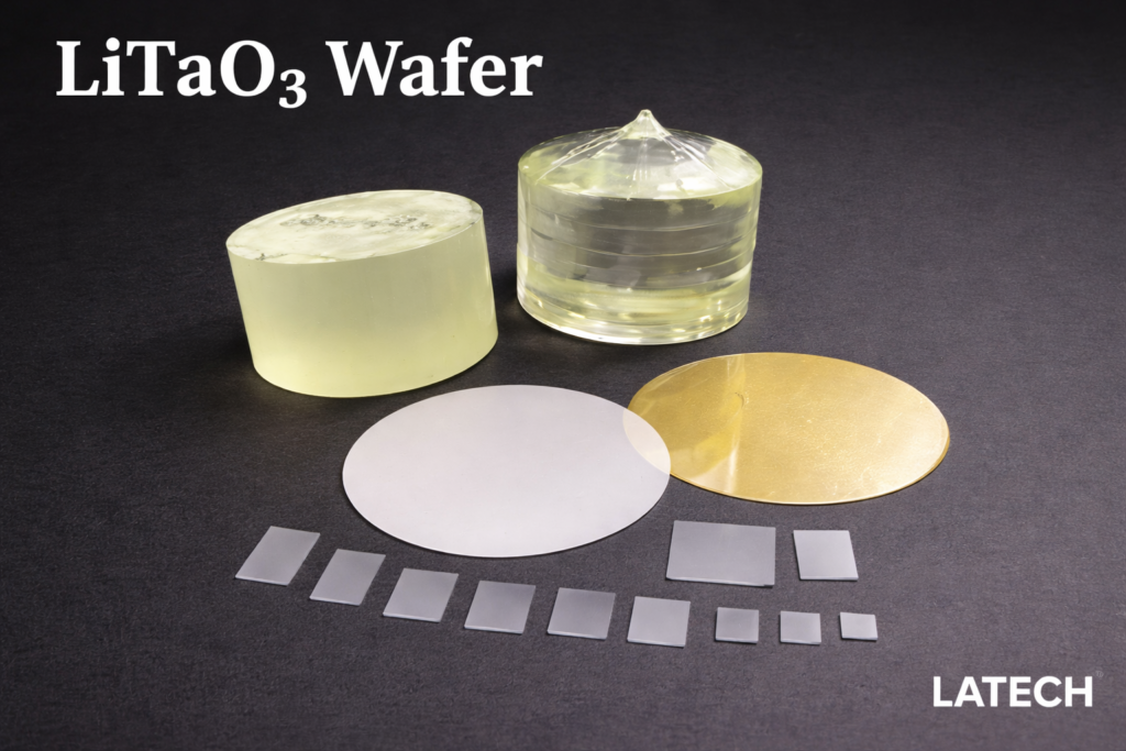
LiTaO₃ Wafer (Lithium Tantalate Substrate)
Wafer
Ternary Wafer
High-performance piezoelectric and electro-optic substrate for SAW devices, sensors, and photonic applications
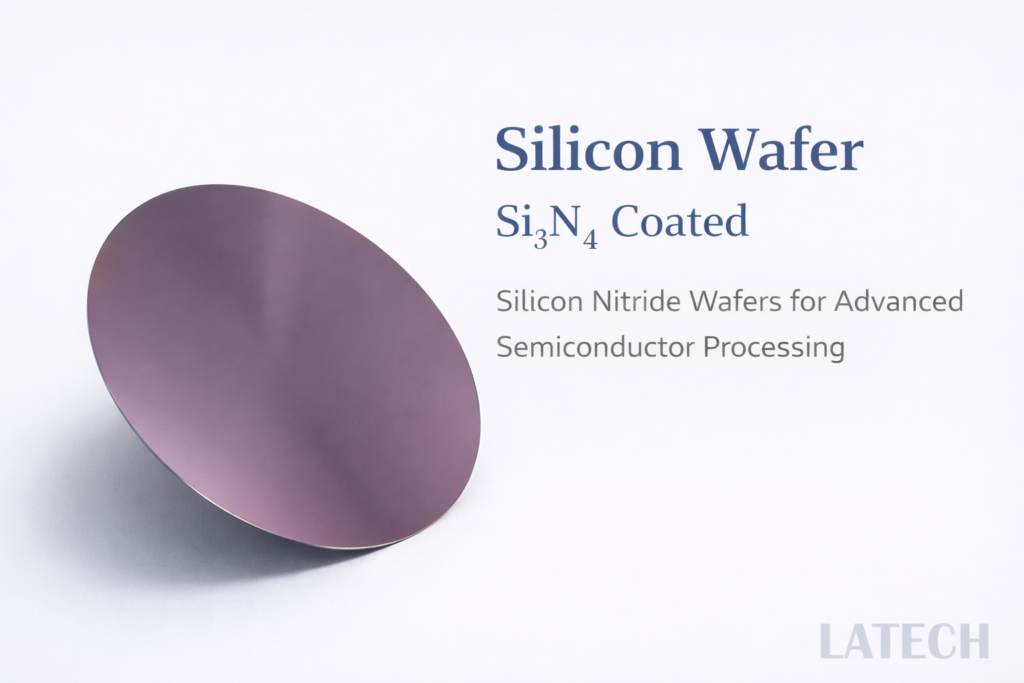
Si₃N₄ Coated Silicon Wafers (Silicon Nitride Wafers)
Elemental Wafer
Wafer
High-performance silicon wafers with silicon nitride coatings for advanced semiconductor and MEMS applications.
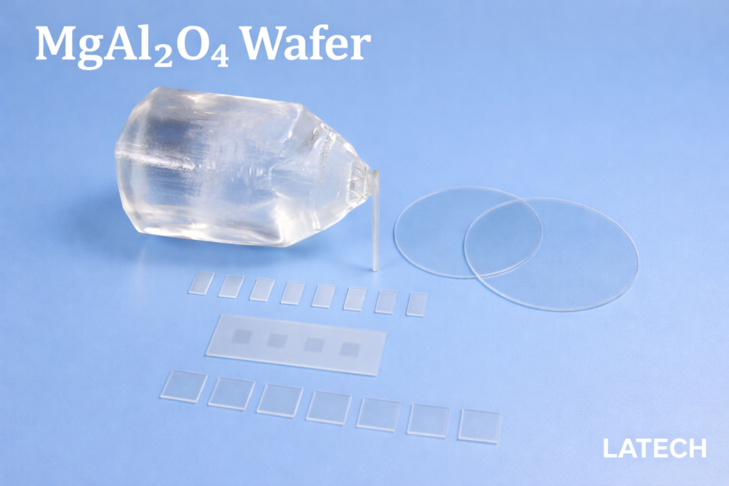
MgAl₂O₄ Wafer (Magnesium Aluminate Spinel Substrate)
Wafer
Ternary Wafer
High-performance insulating spinel substrate for microwave devices, GaN epitaxy, and advanced thin film applications