
MgO Wafer (Magnesium Oxide Substrate)
High-quality MgO wafers for superconducting, epitaxial, and thin-film applications.
Description
🔷 Overview
Magnesium Oxide (MgO) wafers are single-crystal substrates widely used in thin-film deposition, superconducting devices, and oxide electronics.
MgO features a wide bandgap (~7.8 eV) and excellent insulating properties, making it an ideal dielectric substrate for electronic and optical applications.
Its cubic crystal structure (rock-salt) provides excellent lattice matching with a wide range of oxide and nitride materials, enabling high-quality epitaxial growth.
In addition, MgO offers high thermal stability, chemical resistance, and low dielectric loss, making it especially suitable for high-temperature superconducting films, microwave devices, and advanced research applications.
🔷 Key Features
- Wide bandgap (~7.8 eV) for insulating applications
- Excellent lattice matching for oxide thin films
- High thermal stability and high melting point (~2800°C)
- Low dielectric loss for microwave/RF devices
- High optical transparency (UV–IR range)
- Good chemical stability and corrosion resistance
- Suitable for high-temperature and harsh environments
🔷 Specifications
|
Product: |
Single crystal MgO wafer |
|
Purity: |
> 99.99% |
|
Material property: |
Crystal structure: cubic |
|
Lattice constant: a = 4.216 Å |
|
|
Density: 3.98 g/cm3 |
|
|
Melting point: 2800 °C |
|
|
Hardness: 5.5 mohs |
|
|
Coefficient of Thermal expansion: 11.2 x 10⁻⁶ / ℃ |
|
|
Thermal Conductivity: 0.14 @300K ( cal/cm sec degree ) |
|
|
Dielectric Constant: ~ 9.8 @300K |
|
|
Optical transmission: > 90% (200-400 nm), > 98% (500 – 1000 nm) |
|
|
Growth method: Special Arc Melting |
|
|
Dimension: |
• 5 × 5 mm • 5 × 10 mm • 10 × 10 mm • 20 × 20 mm • φ1″ x 0.5mm |
|
Thickness: |
• 0.1 mm • 0.5 mm • 1.0 mm • 2.0 mm • Other sizes customizable |
|
Orientation: |
• <100> ± 0.5° • <110> ± 0.5° • <111> ± 0.5° • other off-angle |
|
Polishing: |
• Fine ground • Single side epi-polished • double side epi-polished |
|
Surface roughness: |
< 0.5 nm |
🔷 Applications
- High-temperature superconducting thin films (HTS)
- Oxide thin-film epitaxy (ferroelectric, magnetic films)
- Microwave and RF devices
- Optical thin films and coatings
- Spintronic and magnetic devices
- Semiconductor research and sensors
🔷 Why Choose MgO
- Excellent substrate for superconducting films (YBCO等)
- Ideal lattice matching for oxide and nitride materials
- Low dielectric loss for high-frequency devices
- High thermal and chemical stability for harsh environments
- Wide optical transparency range for photonic applications
🔷 Customization Options
We support customized MgO wafers based on your requirements:
- Size and thickness
- Orientation (<100>, <110>, <111>)
- Surface polishing (SSP / DSP)
- Epitaxial-grade substrates
- Research-grade substrates
Related Products
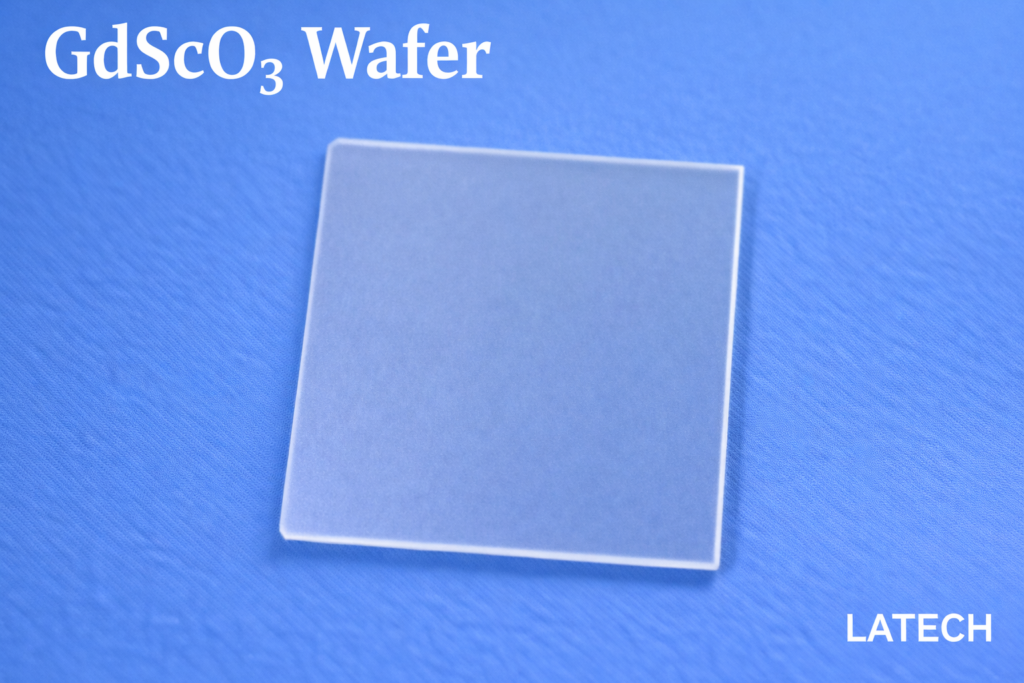
GdScO₃ Wafer (Gadolinium Scandate Wafer)
Wafer
Ternary Wafer
High-quality rare-earth scandate substrate for advanced oxide epitaxy and strain engineering
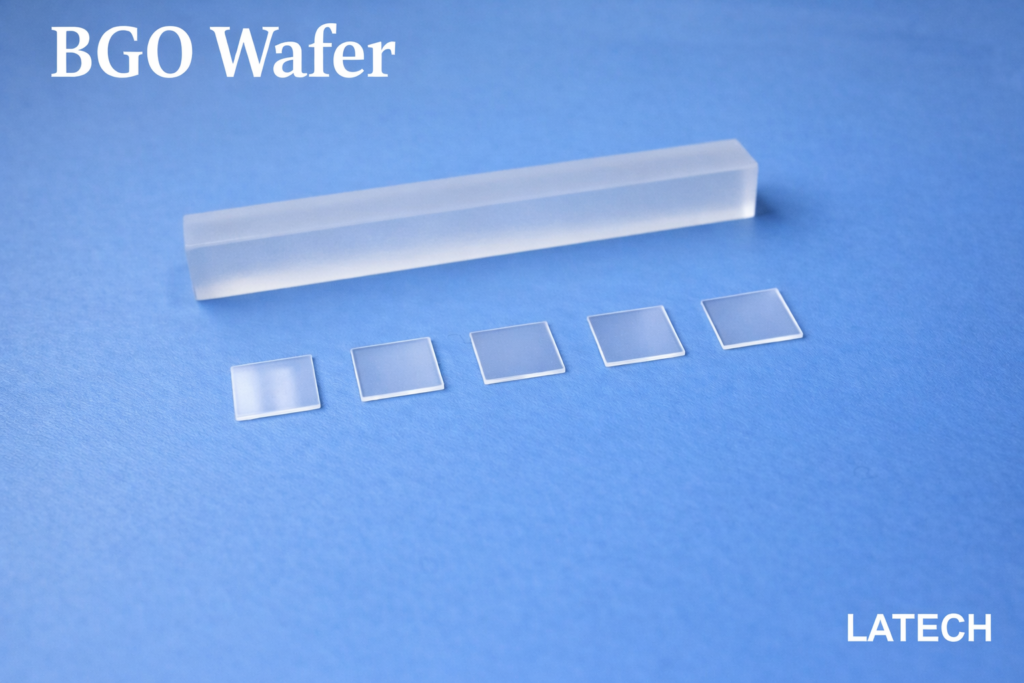
BGO Wafer (Bismuth Germanate, Bi₄Ge₃O₁₂ Wafer)
Wafer
Ternary Wafer
High-density scintillation crystal substrate for radiation detection and optoelectronic applications
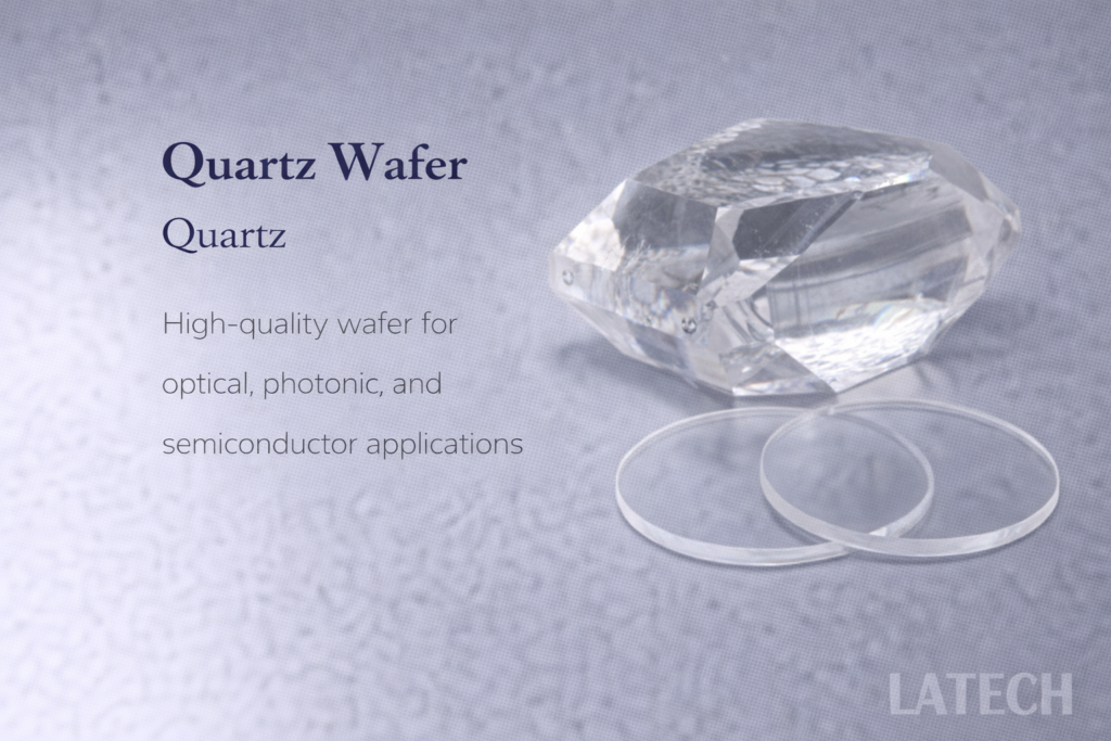
Single Crystal Quartz Wafer (SiO₂ Substrate)
Binary Wafer
Wafer
High-quality single crystal quartz wafers for optical, piezoelectric, and frequency control applications.
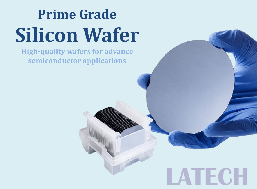
Prime Grade Silicon Wafer
Elemental Wafer
Wafer
High purity monocrystalline silicon substrate for semiconductor and research applications
SiC Wafer (Silicon Carbide Wafer)
Binary Wafer
Wafer
High-performance SiC wafers for power electronics, high-temperature, and high-frequency applications.