
MgF₂ Wafer (Magnesium Fluoride Substrate)
High-quality MgF₂ wafers for UV, optical, and photonic applications.
Description
🔷 Overview
Magnesium Fluoride (MgF₂) wafers are single-crystal optical substrates widely used in ultraviolet (UV), infrared (IR), and photonic applications.
MgF₂ is known for its exceptionally wide optical transmission range (~0.12–7 μm), covering deep ultraviolet to mid-infrared wavelengths, making it one of the most important materials for optical systems and laser applications.
With a low refractive index (~1.37–1.38), MgF₂ is widely used as an anti-reflection material, improving optical transmission efficiency and reducing surface reflection losses.
In addition, MgF₂ exhibits excellent mechanical strength, thermal stability, and resistance to moisture and chemicals, ensuring reliable performance in demanding environments such as aerospace and high-energy laser systems.
🔷 Key Features
- Ultra-wide transmission range (UV to IR, ~0.12–7 μm)
- Low refractive index (~1.37) for anti-reflection applications
- High optical transparency (>90% in UV–IR range)
- Slight birefringence for polarization optics
- High laser damage threshold (suitable for UV lasers)
- Good mechanical strength and durability
- Excellent chemical and moisture resistance
🔷 Specifications
|
Product: |
Single crystal Magnesium Fluoride (MgF2) wafer |
|
Purity: |
> 99.99% |
|
Material property: |
Crystal structure: tetragonal |
|
Lattice constant: a = 4.64 Å, c = 3.06 Å |
|
|
Density: 3.18 g/cm3 |
|
|
Melting point: 1255 °C |
|
|
Hardness: 6 mohs |
|
|
Coefficient of Thermal expansion: 13.7 x 10⁻⁶ / ℃ |
|
|
Transmission Band: 0.12~8.5 um |
|
|
Dielectric constant: 4.87 (para) 5.54 (perp) at 1MHz |
|
|
Thermal Conductivity: 21 (para) 5.54 (perp) W/K.m at 300K |
|
|
Cleavage Plane: <110> |
|
|
Growth method: Bridgeman, Czochralski method |
|
|
Dimension: |
• 5 × 5 mm • 5 × 10 mm • 10 × 10 mm • 20 × 20 mm • Other sizes customizable |
|
Thickness: |
• 0.1 mm • 0.5 mm • 1.0 mm • 2.0 mm • Other sizes customizable |
|
Orientation: |
• <001> ± 0.5° • <100> ± 0.5° • <110> ± 0.5° • <111> ± 0.5° • other off-angle |
|
Polishing: |
• Fine ground • Single side epi-polished • double side epi-polished |
|
Surface roughness: |
< 1 nm |
🔷 Applications
- UV optics and excimer laser systems
- Optical windows, lenses, and prisms
- Anti-reflection coatings for optics
- Infrared spectroscopy systems
- Aerospace and space optical systems
- Photonic and laser devices
🔷 Why Choose MgF₂
- Exceptional UV transmission down to ~120 nm
- Low refractive index ideal for AR coatings
- Broad optical range covering UV to IR
- High durability compared to other optical crystals
- High laser damage threshold for high-energy applications
🔷 Customization Options
We support customized MgF₂ wafers based on your requirements:
- Diameter and thickness
- Crystal orientation
- Optical-grade polishing (SSP / DSP)
- UV-grade or IR-grade substrates
- Coated or uncoated wafers
Related Products
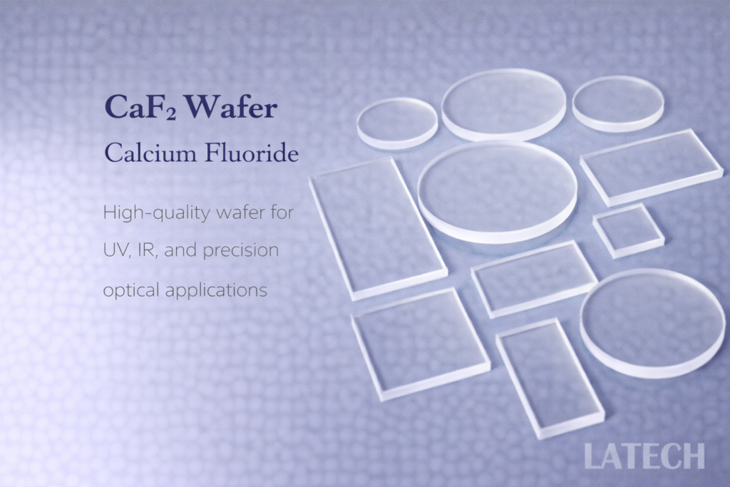
CaF₂ Wafer (Calcium Fluoride Substrate)
Binary Wafer
Wafer
High-quality CaF₂ wafers for UV, IR, and high-precision optical applications.
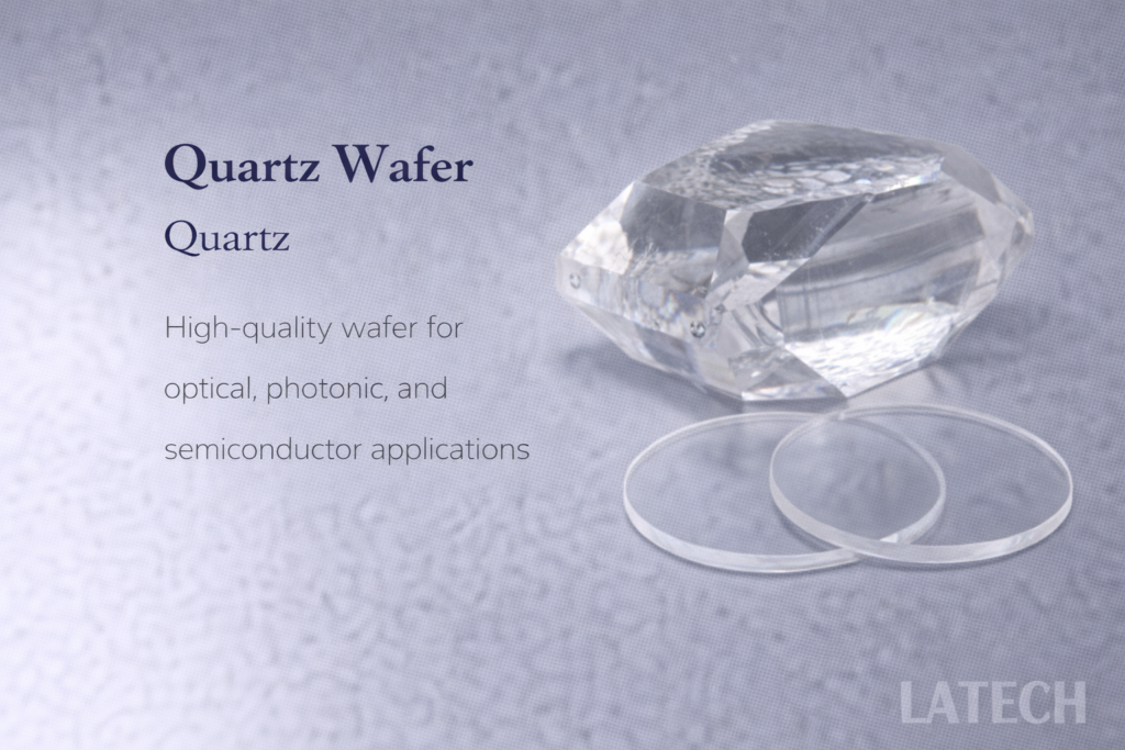
Single Crystal Quartz Wafer (SiO₂ Substrate)
Binary Wafer
Wafer
High-quality single crystal quartz wafers for optical, piezoelectric, and frequency control applications.
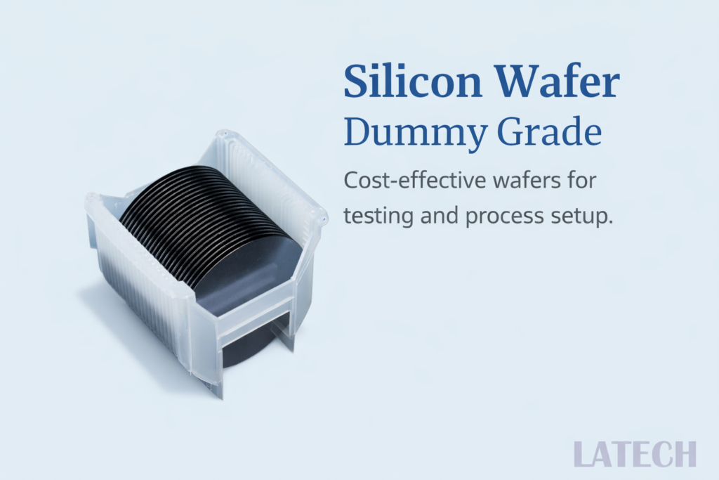
Dummy Grade Silicon Wafer
Elemental Wafer
Wafer
Cost-effective silicon wafer for process testing, equipment calibration, and non-critical applications

DyScO₃ Wafer (Dysprosium Scandate Wafer)
Wafer
Ternary Wafer
High-quality rare-earth scandate substrate for oxide epitaxy and strain engineering
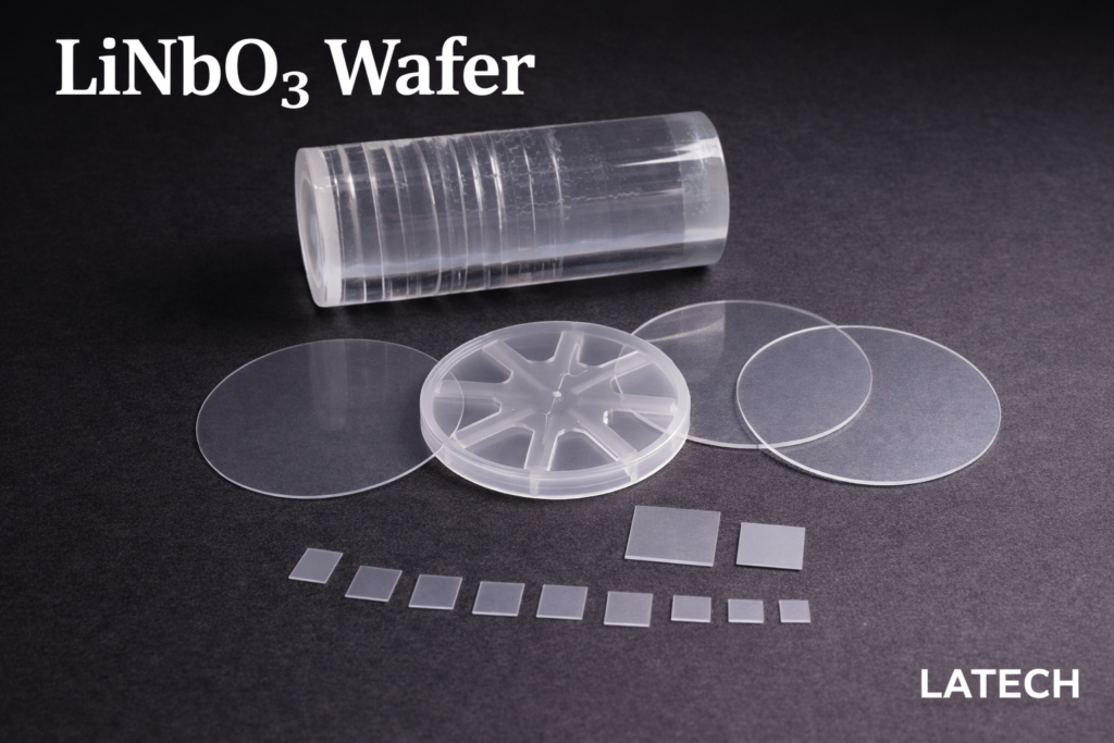
LiNbO₃ Wafer (Lithium Niobate Substrate)
Wafer
Ternary Wafer
High-performance electro-optic and piezoelectric substrate for photonics, modulators, and SAW devices