


SiO₂ Coated Silicon Wafers (Thermal Oxide Wafers)
High-quality silicon wafers with precisely controlled oxide layers for semiconductor and microfabrication applications.
Description
🔷 Description
Silicon wafers with a thermally grown SiO₂ layer are widely used as dielectric and passivation substrates in semiconductor and MEMS processes.
The oxide layer is formed through high-temperature thermal oxidation, ensuring excellent uniformity and stability.
🔷 Key Features
- High-quality thermal oxide (SiO₂) layer
- Excellent thickness uniformity
- Single-side or double-side coating
- Available in prime, test, or dummy grade
- Custom specifications available
🔷 Specifications
| Product: | Si wafer with SiO2 (thermal oxide) layer |
| Production method: | High temperature furnace oxidation of Si wafer |
| Appearance: | Color changes from silver gray to purple/blue after oxidation. |
| Si base wafer: | Oxide layer can be produced on Si wafer of any grade (prime / dummy / solar / etc) |
| SiO2 coating: |
• Oxide layer coated on double sides Oxidation in air naturally produced oxide layer on both sides of the wafers. • Oxide layer coated on single side SiO2 layer on back side (usually non-polished side) can be removed upon request. |
| Oxide layer thickness: | 10 nm up to 10 um |
| Polishing: |
• As-cut wafers without polishing • Single side epi-polished • Double side epi-polished |
🔷 Applications
- Semiconductor fabrication
- MEMS processing
- Dielectric layers
- Surface passivation
- Thin film deposition
Related Products
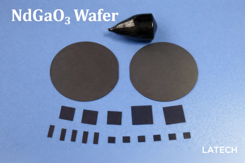
NdGaO₃ Wafer (Neodymium Gallate Substrate)
Ternary Wafer
Wafer
High-quality perovskite oxide substrate for superconducting, magnetic, and epitaxial thin film applications
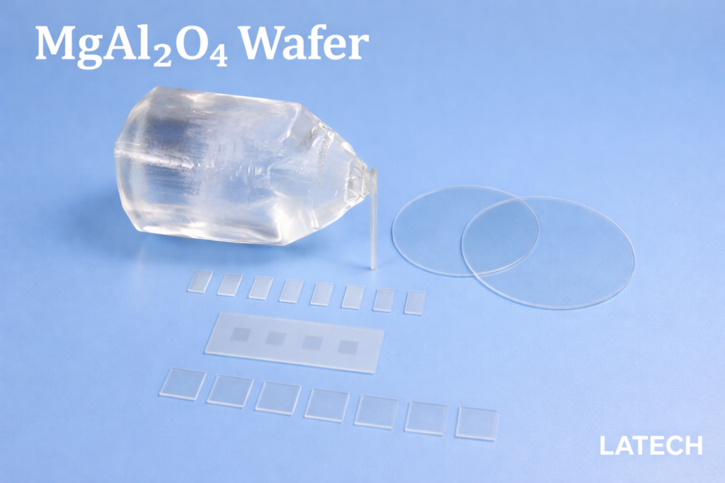
MgAl₂O₄ Wafer (Magnesium Aluminate Spinel Substrate)
Wafer
Ternary Wafer
High-performance insulating spinel substrate for microwave devices, GaN epitaxy, and advanced thin film applications
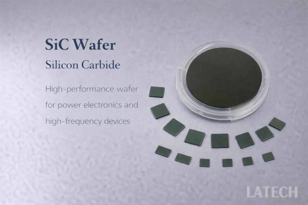
SiC Wafer (Silicon Carbide Wafer)
Binary Wafer
Wafer
High-performance SiC wafers for power electronics, high-temperature, and high-frequency applications.

SrTiO₃ Wafer (Strontium Titanate Wafer)
Wafer
Ternary Wafer
High-quality insulating perovskite oxide substrate for epitaxial growth and advanced oxide thin film applications
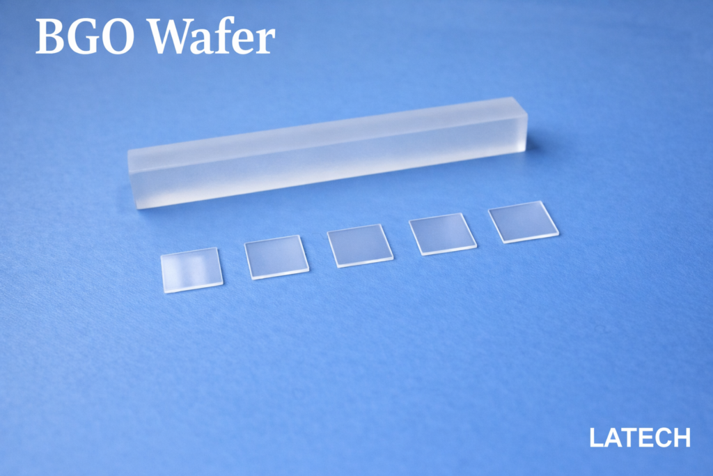
BGO Wafer (Bismuth Germanate, Bi₄Ge₃O₁₂ Wafer)
Wafer
Ternary Wafer
High-density scintillation crystal substrate for radiation detection and optoelectronic applications