
Description
🔷 Product Overview
Solar grade silicon wafers are primarily used in photovoltaic (solar cell) applications, where large-scale production and cost efficiency are critical.
Compared to semiconductor-grade wafers, solar wafers typically have lower purity and less stringent specifications, making them a more economical choice for energy-related applications.
🔷 Key Specifications
| Product: | Silicon (Si) wafer |
| Grade: |
Solar grade Solar wafers are usually polycrystalline wafers produced in industrial scale with fixed conductive type (p-type) and sizes. But we also have solar wafers of both polycrystallnity and monocrystallinity with customized sizes and resistivity for small scale non-standard applications. |
| Purity: |
• 99.999% – 99.99999% (5N – 6N) • Single crystal or polycrystal |
| Dimension: |
Standard size: • 156 × 156 × 0.2 mm Other diameters and thicknesses available • 125 × 125 × 0.2 mm • others |
| Orientation: |
• Polycrystal • For single crystal, we have <100> / <110> / <111> / others |
| Conductive type: |
• p-type • (n-type is also available but is less common) |
| Resistivity: |
Standard resistivity • 1 – 3 Ω·cm Other resistivity available |
| Minority carrier lifetime: |
> 2 usec |
| Polishing: |
• As-cut wafers without polishing • Single side epi-polished • Double side epi-polished |
| Surface roughness: | < 0.5 nm |
| Remarks: | 100 pcs per pack. MOQ 100 pcs |
🔷 Difference from Semiconductor Wafers
| Feature | Solar Grade | Prime Grade |
|---|---|---|
| Purity | Medium (5N–6N) | Ultra-high (9N–11N) |
| Structure | Poly / mono | Mono |
| Surface | Basic | Polished |
| Application | Solar cells | IC / MEMS |
| Cost | Low | High |
🔷 Applications
- Solar cell fabrication
- Photovoltaic research
- Energy materials development
- Teaching and laboratory use
🔷 Key Advantages
- Cost-effective for large-scale use
- Industry-standard dimensions
- Suitable for photovoltaic production
- Available in bulk quantities
Related Products
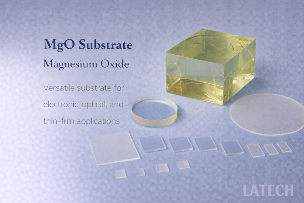
MgO Wafer (Magnesium Oxide Substrate)
Binary Wafer
Wafer
High-quality MgO wafers for superconducting, epitaxial, and thin-film applications.
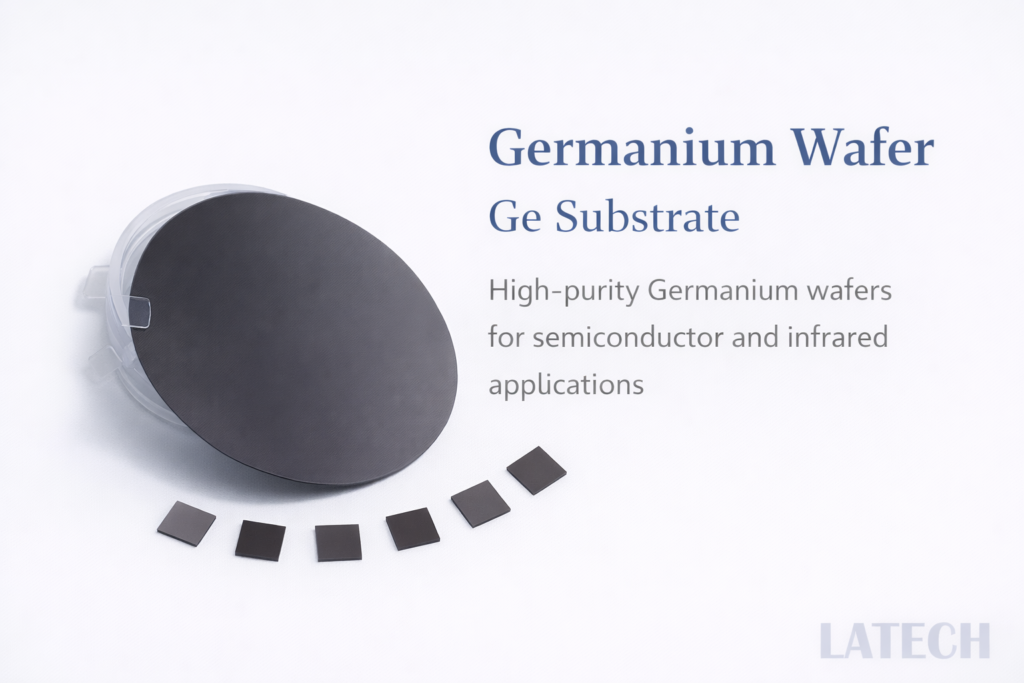
Germanium Wafer (Ge Wafer)
Elemental Wafer
Wafer
High-purity germanium wafers for infrared, optical, and semiconductor applications.
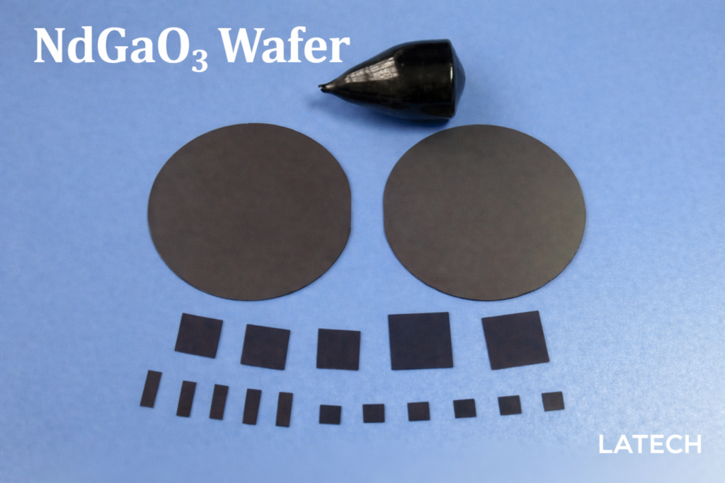
NdGaO₃ Wafer (Neodymium Gallate Substrate)
Wafer
Ternary Wafer
High-quality perovskite oxide substrate for superconducting, magnetic, and epitaxial thin film applications

LiAlO₂ Wafer (Lithium Aluminate Substrate)
Wafer
Ternary Wafer
High-performance substrate for GaN epitaxy, superconducting films, and microwave applications
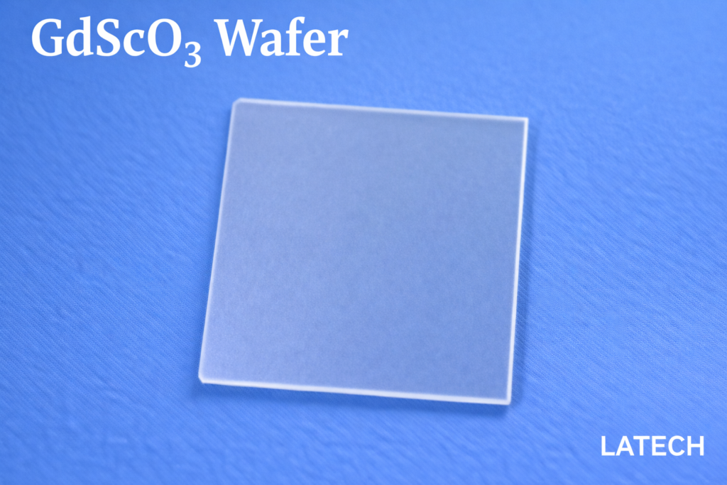
GdScO₃ Wafer (Gadolinium Scandate Wafer)
Wafer
Ternary Wafer
High-quality rare-earth scandate substrate for advanced oxide epitaxy and strain engineering