
GGG Wafer (Gadolinium Gallium Garnet, Gd₃Ga₅O₁₂ Wafer)
High-quality garnet substrate for magnetic thin films and oxide epitaxy
Description
🔷 Overview
GGG (Gadolinium Gallium Garnet, Gd₃Ga₅O₁₂) wafer is a cubic single crystal widely used as a substrate for epitaxial growth of magnetic garnet films such as YIG. It provides excellent lattice matching, high thermal stability, and superior surface quality, making it an ideal choice for spintronic, microwave, and magneto-optical applications.
🔷 Key Features
• Cubic garnet crystal structure
• Excellent lattice matching with YIG (low mismatch ~0.03%)
• High thermal and chemical stability
• Epi-ready surface with ultra-low roughness (< 0.5 nm)
• Low defect density for high-quality thin film growth
🔷 Specifications
| Material: | Gd3Ga5O12 (GGG) |
| Material property: | Crystal structure: Cubic |
| Lattice constant: a =12.376Å | |
| Density: 7.09 g/cm3 | |
| Melting point: 1800 °C | |
| Growth Method: | CZ |
| Dimension: |
• 5 × 5 × 0.5 mm • 10 × 10 × 0.5 mm • Other sizes customizable |
| Orientation: | <100> / <110> / <111> |
| Polishing: | Single side / double side epi-polished |
| Surface roughness: | < 0.5 nm |
🔷 Applications
• YIG (Y₃Fe₅O₁₂) thin film growth
• Spintronics and magnonics devices
• Microwave and RF components
• Magneto-optical devices
• Oxide thin film epitaxy
🔷 Customization Options
• Orientation and off-cut customization
• Thickness and dimension customization
• Double-side polishing (DSP) available
• Epi-ready surface treatment
Related Products
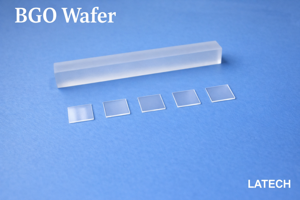
BGO Wafer (Bismuth Germanate, Bi₄Ge₃O₁₂ Wafer)
Ternary Wafer
Wafer
High-density scintillation crystal substrate for radiation detection and optoelectronic applications

ZnO Wafer (Zinc Oxide Substrate)
Binary Wafer
Wafer
High-quality ZnO wafers for optoelectronic, piezoelectric, and thin-film applications.

TiO₂ Wafer (Titanium Dioxide Substrate)
Binary Wafer
Wafer
High-quality TiO₂ substrates for optical, photonic, and thin-film applications.
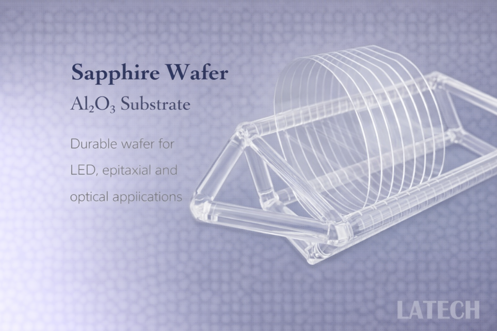
Sapphire Wafer (Al₂O₃ Substrate)
Binary Wafer
Wafer
High-quality sapphire wafers for LED, epitaxial, optical, and semiconductor applications.
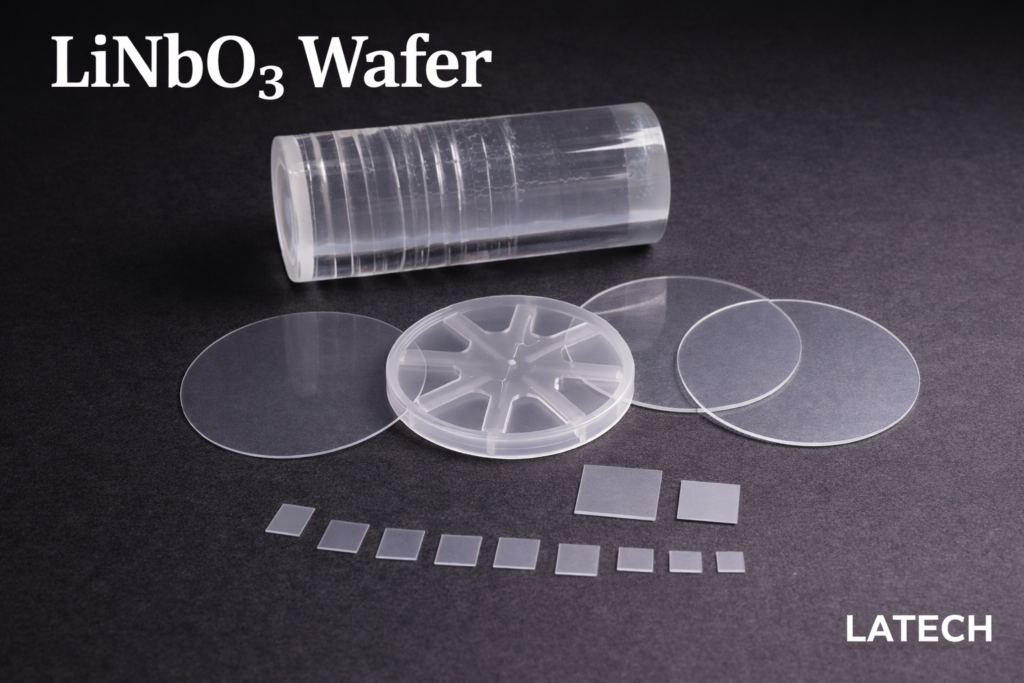
LiNbO₃ Wafer (Lithium Niobate Substrate)
Wafer
Ternary Wafer
High-performance electro-optic and piezoelectric substrate for photonics, modulators, and SAW devices