


ZnO Wafer (Zinc Oxide Substrate)
High-quality ZnO wafers for optoelectronic, piezoelectric, and thin-film applications.
Description
🔷 Overview
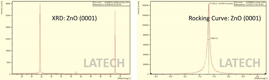
Zinc Oxide (ZnO) wafers are II–VI compound semiconductor substrates widely used in optoelectronics, piezoelectric devices, and thin-film applications.
ZnO features a wide bandgap (~3.2–3.37 eV), making it suitable for ultraviolet (UV) optoelectronic devices such as LEDs and photodetectors.
In addition, ZnO exhibits strong piezoelectric properties and high exciton binding energy, enabling high-performance sensors, acoustic devices, and nanoscale electronics.
ZnO substrates are also widely used for epitaxial growth of nitride-based and oxide thin films, offering excellent lattice compatibility and surface quality.
🔷 Key Features
- Wide bandgap (~3.2–3.37 eV) for UV applications
- Strong piezoelectric properties for sensors and MEMS
- High exciton binding energy for efficient optical emission
- Good optical transparency in visible range
- Suitable for thin-film epitaxy and device fabrication
- High chemical stability and non-toxic material
- Available in multiple orientations and polishing options
🔷 Specifications
| Product: | Single crystal zinc oxide (ZnO) wafer |
| Purity: | > 99.99% |
| Material property: | Crystal structure: hexagonal |
| Lattice constant: a = 3.252 Å, c = 5.313 Å | |
| Bandgap: 3.37 eV (300 K) | |
| Hardness: 4 Mohs | |
| Melting point: 1975 °C (decompose) | |
| Growth Method: | Hydrothermal |
| Dimension: |
• 5 × 5 × 0.5 mm • 10 × 10 × 0.5 mm • Other sizes customizable |
| Orientation: | <0001> |
| Conductive type: | Native n-type semiconductor |
| Polishing: | Single side / double side epi-polished |
| Surface roughness: | < 0.5 nm |
🔷 Applications
- UV LEDs and photodetectors
- Piezoelectric devices and sensors
- Surface acoustic wave (SAW) devices
- Transparent electronics and thin films
- Nitride and oxide epitaxial growth
- MEMS and nanoscale devices
🔷 Why Choose ZnO
- Wide bandgap enables UV optoelectronic applications
- Strong piezoelectric effect for sensing applications
- High transparency in visible spectrum
- Environmentally friendly and non-toxic material
- Excellent substrate for oxide and nitride thin films
🔷 Customization Options
We support customized ZnO wafers based on your requirements:
- Size and thickness
- Orientation (<0001>, <10-10>, <11-20>)
- Doping type
- Surface polishing (SSP / DSP)
- Epitaxial-ready wafers
Related Products

TiO₂ Wafer (Titanium Dioxide Substrate)
Binary Wafer
Wafer
High-quality TiO₂ substrates for optical, photonic, and thin-film applications.
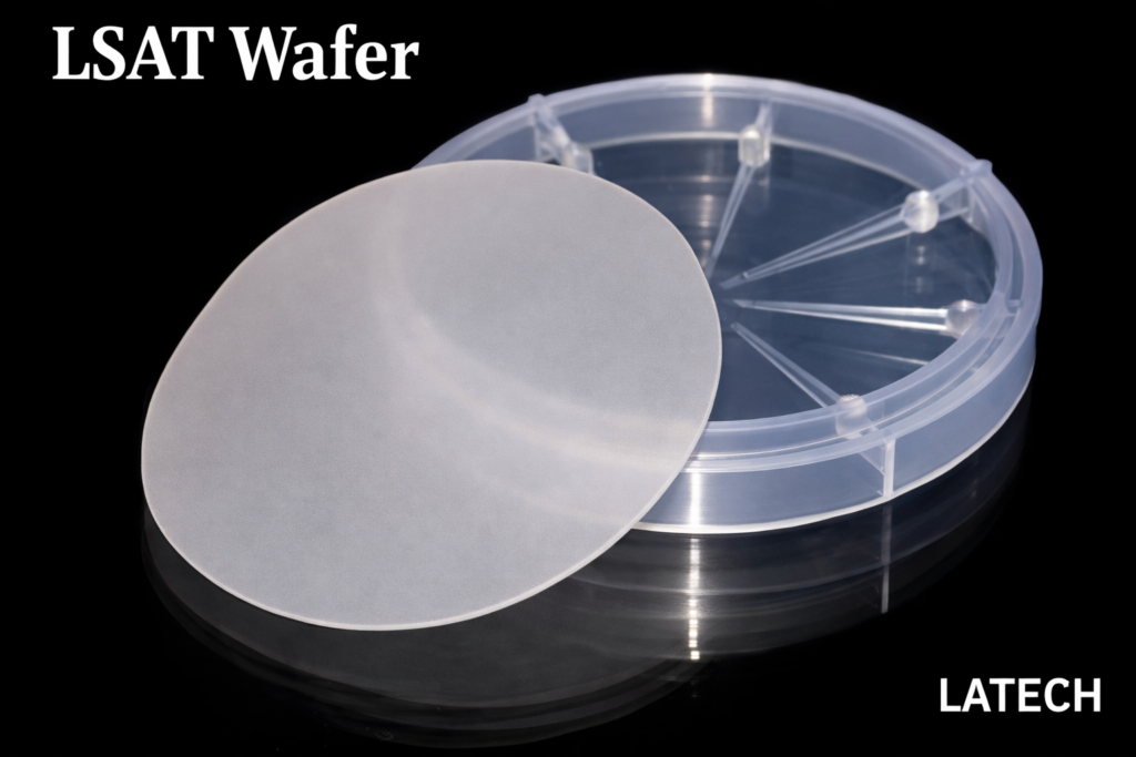
LSAT Wafer
Wafer
Other Wafers
Lattice-matched perovskite substrate for oxide epitaxy and superconducting thin films
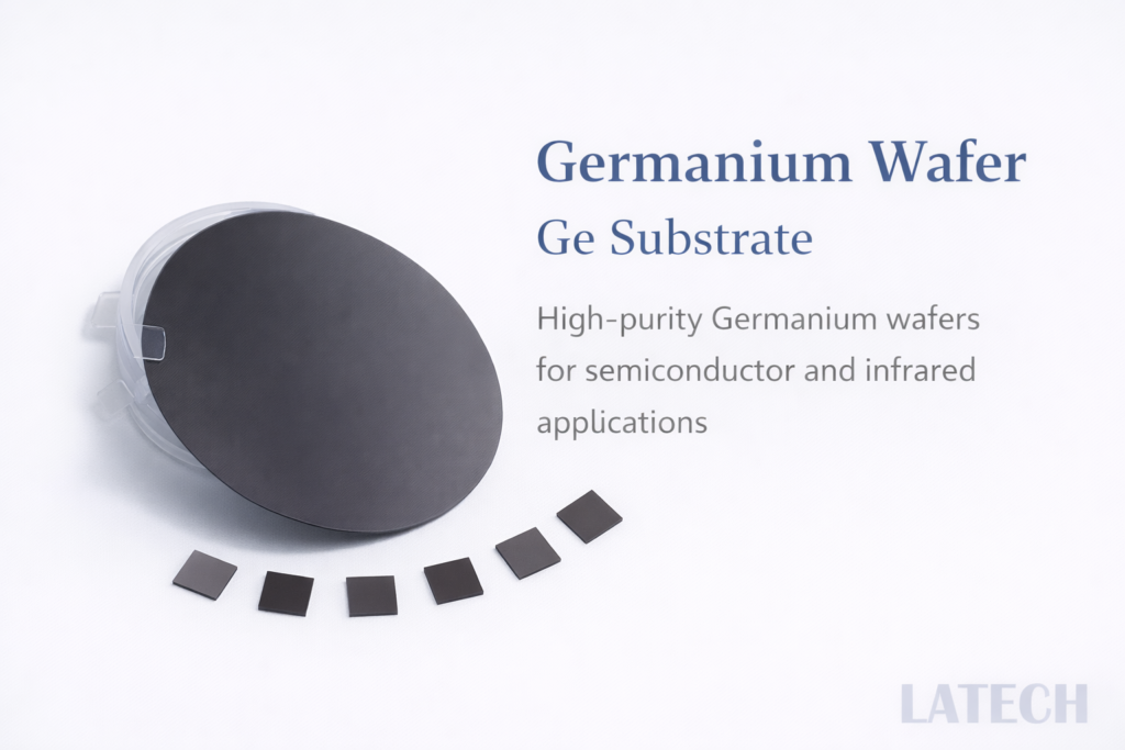
Germanium Wafer (Ge Wafer)
Elemental Wafer
Wafer
High-purity germanium wafers for infrared, optical, and semiconductor applications.
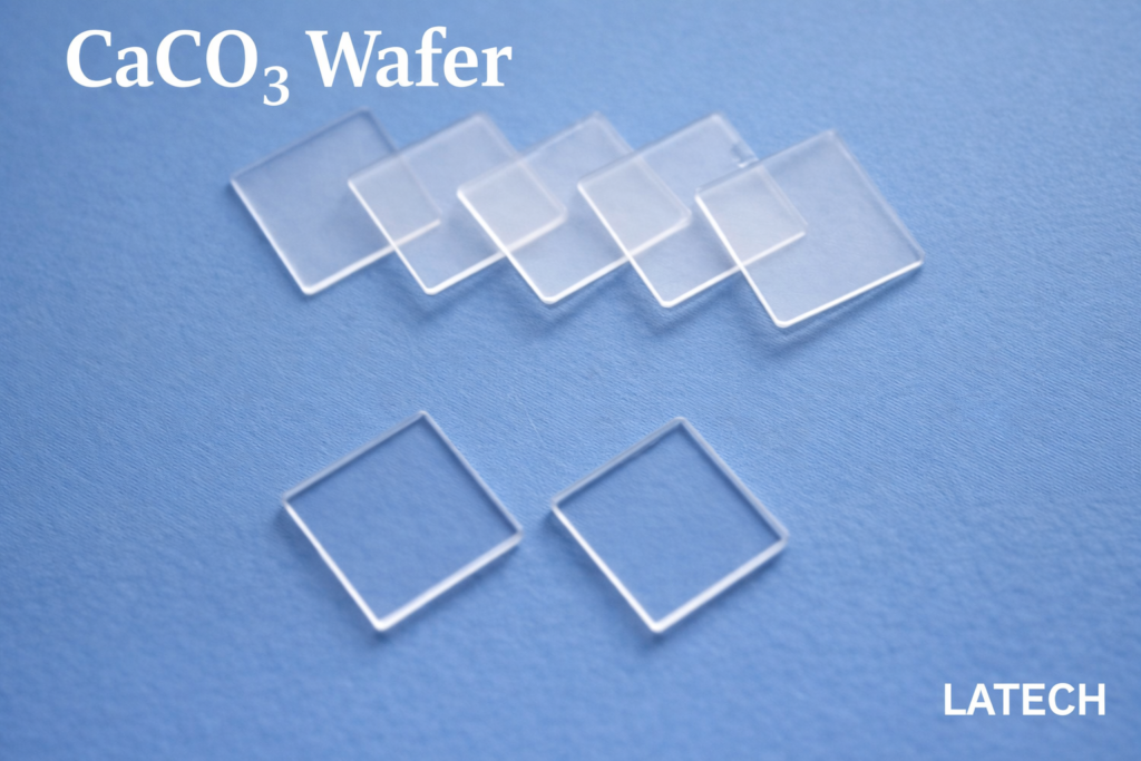
CaCO₃ Wafer (Calcium Carbonate Wafer)
Wafer
Ternary Wafer
High birefringence optical crystal substrate for polarization and photonic applications
GdScO₃ Wafer (Gadolinium Scandate Wafer)
Wafer
Ternary Wafer
High-quality rare-earth scandate substrate for advanced oxide epitaxy and strain engineering